Band Gaps are some set of Rules
In a regular periodic crystal lattice, electrons as the carriers of electrical current are not allowed to move around freely. Instead, they have to obey certain rules enforced by quantum mechanics.
As a consequence, electrons have to occupy so-called “energy bands” which are separated from each other by small or large “band gaps”.
What is Conduction Band and Valance Band
In the language of solid state physics, these two storey's are called “valence band” and “conduction band”, respectively.
In the same way, electrons in a solid crystal have to obey the quantum-mechanical “exclusion principle” formulated by the famous physicist Wolfgang Pauli.
Now that the blueprints of our semiconductor building and the basic rules for its inhabitants have been defined, let us start to occupy this building with people.
Further inhabitants can only occupy the first floor, where they again have sufficient room to move about. As a consequence, the overall cargo stream through the building will again start to increase, reach a maximum, and eventually come to an end when also the first floor is fully occupied.
A. What is a Conductor?
Crystals in which energy bands are only partially filled will belong to the group of electrical conductors, since their electrons can move more or less freely through the crystal lattice.
If, on the other hand, all energy bands are fully occupied or completely empty, no electrical current can pass through the crystal at all and we are dealing with an electrical insulator.
Which situation will be encountered for a given solid crystal depends on how many electrons per atom are available to occupy the energy bands of the crystal.
For example, almost all metals are very good electrical conductors due to a half-filled conduction band, whereas metal oxides very often are good insulators with a completely filled valence band and an empty conduction band.
B. What is a Semi-Conductor?
Semiconductors are solids which are able to pass an electrical current much better than insulators, but at the same time not as efficiently as an electrical conductor. Obviously, semiconductors are solids in which for one reason or the other a few of the many tiles on the ground floor remain empty or a few of the conduction band tiles are occupied, or both.
C. What is an Insulator?
Insulator, where all tiles in the ground floor are occupied by exactly one inhabitant and all tiles in the first floor are empty. Thus, no charge transport can occur.
Doping and the Band Theory
In the analogue of our semiconductor building, doping can be achieved by adding special tiles with the following properties.
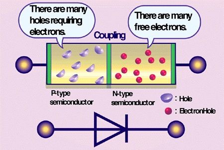
Therefore, doping of a semiconductor crystal with acceptor atoms is referred to as “p-type” doping (“p” as in positive).
2. Donor Ion and Electron Theory
The second possibility to induce controlled electrical conduction in an insulator is the doping with donor impurities.
In a regular periodic crystal lattice, electrons as the carriers of electrical current are not allowed to move around freely. Instead, they have to obey certain rules enforced by quantum mechanics.
As a consequence, electrons have to occupy so-called “energy bands” which are separated from each other by small or large “band gaps”.
 |
| Band Diagram |
What is Conduction Band and Valance Band
This situation can be compared to a two storey building consisting of a ground floor and a first floor.
 |
| Energy Band analogy |
In the language of solid state physics, these two storey's are called “valence band” and “conduction band”, respectively.
Both floors are covered by a well-ordered array of quadratic tiles, representing the periodic lattice of atoms in a semiconductor crystal.
The movement of electrons in a crystal is then analogous to the movement of inhabitants in our building, whose most important purpose it is to transport “charge” from one end of the building to the other end. (Inhabitant=The person who is staying in the House)
The inhabitants of our “semiconductor house” have to obey one additional important rule: at no time more than one inhabitant is allowed to occupy the space of a given tile!
In the same way, electrons in a solid crystal have to obey the quantum-mechanical “exclusion principle” formulated by the famous physicist Wolfgang Pauli.
Now that the blueprints of our semiconductor building and the basic rules for its inhabitants have been defined, let us start to occupy this building with people.
Analogy for the Band Concept
At first, all inhabitants can be accommodated on the ground floor, where they can move around more or less freely and transport their cargo across the building. This leads to a steady increase of the amount of cargo transported through the building, until the occupancy of the ground floor has increased so much that the inhabitants start to hinder one another on their way. Eventually, the stream of cargo will come to a complete stop, once all tiles in the ground floor are occupied by an inhabitant, so that nobody is able to move any more.
Further inhabitants can only occupy the first floor, where they again have sufficient room to move about. As a consequence, the overall cargo stream through the building will again start to increase, reach a maximum, and eventually come to an end when also the first floor is fully occupied.
A. What is a Conductor?
Crystals in which energy bands are only partially filled will belong to the group of electrical conductors, since their electrons can move more or less freely through the crystal lattice.
If, on the other hand, all energy bands are fully occupied or completely empty, no electrical current can pass through the crystal at all and we are dealing with an electrical insulator.
Which situation will be encountered for a given solid crystal depends on how many electrons per atom are available to occupy the energy bands of the crystal.
For example, almost all metals are very good electrical conductors due to a half-filled conduction band, whereas metal oxides very often are good insulators with a completely filled valence band and an empty conduction band.
B. What is a Semi-Conductor?
Semiconductors are solids which are able to pass an electrical current much better than insulators, but at the same time not as efficiently as an electrical conductor. Obviously, semiconductors are solids in which for one reason or the other a few of the many tiles on the ground floor remain empty or a few of the conduction band tiles are occupied, or both.
C. What is an Insulator?
Insulator, where all tiles in the ground floor are occupied by exactly one inhabitant and all tiles in the first floor are empty. Thus, no charge transport can occur.
Doping and the Band Theory
In the analogue of our semiconductor building, doping can be achieved by adding special tiles with the following properties.
1. Acceptor Ion and Hole Theory
As a first example, so-called “acceptor tiles” can be added to the ground floor. These acceptor tiles have the unpleasant property of swallowing exactly one inhabitant of the fully occupied ground floor, thus creating a “hole” in the overall occupancy.
 |
| Holes and Electrons in an Atom |
This allows the other inhabitants of the ground floor to move again. The hole created by the acceptor-tiles also will move at the same time, however in the opposite direction as compared to the inhabitants. In the same way, acceptor atoms incorporated into a semiconductor crystal will create a hole in the occupancy of the valence band, which will act as a “missing electron” and, thus, as a positively charged particle in electrical transport.
 |
| Valance Band with Holes |
Therefore, doping of a semiconductor crystal with acceptor atoms is referred to as “p-type” doping (“p” as in positive).
2. Donor Ion and Electron Theory
The second possibility to induce controlled electrical conduction in an insulator is the doping with donor impurities.
In our semiconductor building, such “donor tiles” bring along one additional inhabitant, who has to occupy a free tile in the first floor, since all tiles of the ground floor are already occupied. Accordingly, donor atoms added to a semiconductor crystal will provide additional electrons in the conduction band, which contribute to electronic charge transport in the expected way (“n-type” doping by additional negatively charged electrons).
 |
| Conduction Band with Extra Electrons |
3. Effect of Thermal Energy and Light Energy
There is yet another way to produce additional holes in the valence band or electrons in the conduction band of a semiconductor without doping, namely by providing external energy in the form of heat or light.
We all know from our own experience that it takes energy to walk up the stairs from the ground floor to the first floor.
The same holds for the electrons in a semiconductor: electrons in the conduction band (first floor) have a higher energy than electrons in the valence band (ground floor). This difference in energy is determined by the band gap of the semiconductor.
Since electrons are lazy, they prefer to stay on the ground floor. In order to move up to the first floor, they have to be stimulated by an external influence. One possibility is provided by the thermal movement of the atoms. At low temperatures, atoms are frozen at their lattice sites, but at higher temperatures they start to wiggle more and more and to push the electrons around.
 | |||||||||||
In the analogue of our semiconductor building, the thermal motion of the atoms can be visualized by a staircase leading from the ground floor to the first floor. The thermal motion of the atoms will push the electrons upwards step by step. The larger the band gap of the semiconductor, the longer the staircase and the smaller the number of electrons which actually make it all the way up to the first floor.
However, in every well-planned building, there is also another possibility to reach the upper floors more easily: an elevator. In semiconductors, the job of the elevator is done by the elementary particles of light, the photons.
If such a flash of light hits a semiconductor, it can directly elevate an electron from the valence band up to the conduction band. The stronger the light beam that falls onto the semiconductor, the more often the photon elevator will make the trip between the two floors, each time taking an electron with it.
Recombination
But also the other direction of electron transport is possible: electrons in the conduction band can return to the valence band, if there is a hole to accommodate the returning electron. This process is called “recombination”.
 |
| Recombination in a Diode |
To do this, the electrons can either take the staircase down, giving their energy back to the atoms, or they can take the photon elevator. Then, each time the elevator doors open in the valence band and an electron recombines with a hole, an elementary flash of light is emitted by the semiconductor.
The energy of the emitted photon is the same as the band gap of the semiconductor. Semiconductors with a small band gap emit red photons, whereas semiconductors with a large band gap emit blue photons.
(Courtesy: http://www.wsi.tum.de)
Chem Academy Offering IIT JAM Coaching in Jaipur and Best coaching institute for IIT JAM Physics. You can Get Complete Information about Best coaching for IIT Jam Physics and Chemistry. Chem Academy is known as Best IIT JAM Coaching in Jaipur/India. Classroom coaching for JAM 2020 and IIT JAM Physics classes in Jaipur now Admission Open. IIT JAM physics coaching in jaipur This blog is honestly beneficial concerning all educational understanding I earned. It covered a wonderful region of issue that may help some of needy humans. everything cited here is obvious and without a doubt beneficial.
ReplyDeleteSimple wristbands, big impact on event security. Wristbands247
ReplyDeleteLove the colors and design on these wristbands. custom wristbands
ReplyDeleteWristbands help improve event security. view wristband options
ReplyDelete