Friday, August 03, 2012

Binary decoder

A decoder is a multiple-input, multiple-output logic circuit that converts coded inputs into coded outputs, where the input and output codes are different; e.g. n-to-2n, BCD decoders. Enable inputs must be on for the decoder to function, otherwise its outputs assume a single "disabled" output code word.Decoding is necessary in applications such as data multiplexing, 7 segment display and memory address decoding. Figure below shows the pseudo block of a decoder.


Basic Binary Decoder

AND gate can be used as the basic decoding element, because its output is HIGH only when all its inputs are HIGH. For example, if the input binary number is 0110, then, to make all the inputs to the AND gate HIGH, the two outer bits must be inverted using two inverters as shown in figure below.


Binary n-to-2n Decoders


A binary decoder has n inputs and 2n outputs. Only one output is active at any one time, corresponding to the input value. Figure below shows a representation of Binary n-to-2n decoder


2-to-4 Binary Decoder

A 2 to 4 decoder consists of two inputs and four outputs, truth table and symbols of which is shown below.

Truth table

X
Y
F0
F1
F2
F3
0
0
1
0
0
0
0
1
0
1
0
0
1
0
0
0
1
0
1
1
0
0
0
1

           Symbol
                                          
                               Using k-map we can do the minimization of truth table.
               Circuit


Thursday, August 02, 2012

Schmitt Oscillator

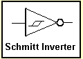
The SCHMITT TRIGGER INVERTER is an INVERTER with a SCHMITT TRIGGER input.

Symbol


It is basically a GATE and can be used as an INVERTER. But the Schmitt Trigger input gives it a lot more features.
The Schmitt Trigger Inverter is shown on the left and the Schmitt symbol must be included to show it is not an ordinary inverter.

It can be used as an Inverter, an oscillator, a Buffer as well as other "Building Blocks." It all depends on the surrounding components.


HOW THE SCHMITT OSCILLATOR WORKS?

Suppose the input is LOW. The output will be HIGH. The voltage across the resistor will cause current to flow through it and charge the capacitor. When the voltage on the capacitor reaches 67% of rail voltage, the gate will change state.
The energy in the capacitor will "bleed" through the resistor and the voltage across the capacitor will gradually fall. When it reaches 32% of rail voltage, the gate will change state.


Hardwork Can Never Ever Fails..
Best luck..


Astable Multivibrator

Transistorised Astable Multivibrator is a cross coupled transistor network capable of producing sharp continuous square wave. It is free running oscillator or simply a regenerative switching circuit using positive feedback. Astable Multivibrator switches continuously between its two unstable states without the need for any external triggering. Time period of Astable multivibrator can be controlled by changing the values of feedback components such as coupling capacitors and resistors.


Astable Multivibrator working


Working:

  • Assume anyone of the transistors Q1 or Q2 turns ON due to parameter variation or due to some switching transients, let it be Q1.
  • Then the collector voltage of Q1=Vce(sat)=0.2V, it is cross coupled to base terminal of Q2 through C1, then Q2 remain in OFF state.
  • During Q1 ON, the current path through R1 charges the capacitor C1, the capacitor C1 voltage is coupled to base of transistor Q2.
  • While charging of C1, when the capacitor voltage exceeds 0.7V, Q2 become turns ON.
  • As soon as Q2 ON, its collector voltage falls to Vce(sat)=0.2V, it is coupled to base terminal of Q1 then Q1 become OFF.
  • At the same time capacitor C2 starts charging through R2, when the C2 voltage exceeds 0.7 V, Q1 turns ON due to cross coupling.
  • This process continues.


Hardwork Can Never Ever Fails...
Best Luck...


What is Blu-ray Disc?

Blu-ray Symbol


Blu-ray Disc (or BD) is an optical disc storage medium just as DVDs and CDs are but it is capable of much higher capacities of 50GB and more.
BD utilises a blue laser (which is actually violet) which uses a much shorter wavelength which is why it can store so much more than DVD.


Optical discs store information with the use of pits and lands which are lined up in a long spiralling track which starts near the centre of the disc and travels outwards. With BD, the pits are smaller, V-shaped and closer together. This allows for more to be fitted onto the disc.

Types of BD ROM

BD-ROM: similar to DVD-ROM and CD-ROM, which must be produced from a pump in the factory.
BD-R: disc can be written once.
BD-RE: Can rewritable discs. (Re-recordable) and writing / remove the disc similar to DVD-RW and CD-RW BD-RE by using substances that change the status of tiered storage. When this is shot with a laser to change the status of the material back and forth a thousand times.

Evolution of Secondary Storage media


Cathode Ray Tube

Click on the link below to see the animation of cathode ray tube.

ANIMATION

Sinusoidal Oscillator

Block Diagram of Oscillator

Before explaining the block diagram of an oscillator, let us recall the concept of positive feedback amplifier. All of you know that positive feedback amplifier consists of amplifier having gain of ‘A’ and feedback circuit with gain of ‘β’. Here, a part of output is fed back to input through feedback circuit. The signal which is fed back is added to the input signal using summer ‘Σ ’ and output of the summer acts as an actual input signal to the amplifier. The figure shows the block diagram of the oscillator. The difference between positive feedback amplifier and oscillator is that, in oscillator, there is no need of external input signal. To start the oscillations, output signal must be fed back in proper magnitude and phase.


Fig: Blockdiagram of Oscillator 
 For Replay click again on 'Click here to Start Animation'


Principle of Oscillators
An oscillator consists of an amplifier and a feedback network. Now, let us see which basic components are required to obtain oscillations.
'Active device' either Transistor or Op Amp is used as an amplifier.
'Feedback circuit' with passive components such as R-C or L-C combinations .

To start the oscillation with the constant amplitude, positive feedback is not the only sufficient condition. Oscillator circuit must satisfy the following two conditions known as Barkhausen conditions:

1. The first condition is that the magnitude of the loop gain (Aβ) must be unity. This means the product of gain of amplifier 'A' and the gain of feedback network 'β' has to be unity.

2. The second condition is that the phase shift around the loop must be 360° or 0°. This means, the phase shift through the amplifier and feedback network has to be 360° or 0°.


How Oscillations are initiated at First?

We have stated that oscillators do not require any external input. This means an oscillator's output feeds its own input and it must satisfy the two essential conditions to start oscillations. Here, you might be eager to know, from where the starting voltage comes. All of you are aware that every resistor has certain free electrons. At room temperature these free electrons move randomly and generate a noise voltage across the resistor due to collisions. This voltage is also known as thermal noise voltage. Hence, the resistor acts as small ‘ac’ voltage source. When power supply is turned on, for the first time this small ac noise voltage gets amplified and appears at the output terminal. This amplified output is applied to feedback circuit and output of feedback circuit is fed back to the amplifier as an input. It is again amplified by amplifier and fed back to input through feedback circuit. This process is repeated and at one particular frequency, circuit satisfies the necessary conditions to start oscillation. Using proper feedback components, it is possible to select the particular frequency.


Fig: How Oscillations are initiated 
 For Replay click again on 'Click here to Start Animation'

ASICs vs FPGA


FPGA
ASIC
Definition
A semiconductor device containing programmable logic components called "logic blocks", and programmable interconnects. Logic blocks can be programmed to perform the function of basic logic gates such as AND, and XOR, or more complex combinational functions such as decoders or mathematical functions.
Definition
An integrated circuit designed for a particular use, rather than intended for general-purpose use. Processors, RAM, ROM, etc are examples of ASICs.

Speed
Less speed.
Speed
ASIC rules out FPGA in terms of speed. As ASIC are designed for a specific application they can be optimized to maximum, hence we can have high speed in ASIC designs. ASIC can have hight speed clocks.

Cost
FPGAs are cost effective for small applications.
Cost
For complex and large volume designs (like 32-bit processors) ASIC products are cheaper.
Size/Area
FPGA contains lots of LUTs, and routing channels which are connected via bit streams(program). As they are made for general purpose and because of re-usability. They are in-general larger designs than corresponding ASIC design.
Size/Area
 Optimised , so smaller
Power
FPGA designs consume more power than ASIC designs. The unwanted circuitry results in wastage of power. FPGA wont allow us to have better power optimization.
Power
When it comes to ASIC designs we can optimize them to the fullest.

Time to Market
FPGA designs will take less time, as the design cycle is small when compared to that of ASIC designs.
Time to Market
ASIC designs will take more time
Type of Design
It is not possible to design mixed signal designs or only analog designs using FPGA chips.

Type of Design
ASIC can have mixed-signal designs, or only analog designs
Customization
FPGA has less customization.
Customization
ASIC has the upper hand when comes to the customization. The device can be fully customized as ASICs will be designed according to a given specification.
Prototyping
Because of re-usability of FPGAs, they are used as ASIC prototypes. ASIC design HDL code is first dumped onto a FPGA and tested for accurate results. Once the design is error free then it is taken for further steps. Its clear that FPGA may be needed for designing an ASIC.


Non Recurring Engineering/Expenses
NRE refers to the one-time cost of researching, designing, and testing a new product. No such thing is associated with FPGA. Hence FPGA designs are cost effective.

Non Recurring Engineering/Expenses
NRE  is generally associated with ASICs.
Design Cycle 
Due to software that handles much of the routing, placement, and timing, FPGA designs have smaller design cycle than ASICs.

Design Cycle 
ASICs have larger design cycle.
More Predictable Project Cycle
Due to elimination of potential re-spins, wafer capacities, etc. FPGA designs have better project cycle.


Tools
Tools which are used for FPGA designs are relatively cheaper than ASIC designs.


Re-Usability
A single FPGA can be used for various applications, by simply reprogramming it (dumping new HDL code). By definition ASIC are application specific cannot be reused.


TDMA Vs FDMA Vs CDMA


Consider an analogy.

There are 20 people inside a room. They want to communicate each other. Assume one to one communication. What are the methods we can follow, so that everyone can communicate each other?

TDMA- Each pair will get 30 seconds to communicate. All pair should wait for their turn. They can speak only when their turn comes. What is the disadvantage of the system? Others are wasting their time when a particular pair is speaking. This is equivalent to Time Division Multiple Access.

FDMA- Each pair should communicate in different pitches. One pair one pitch other in some another pitch. The advantage is that, no one is wasting their time for others, but they must have the ability to speak in different pitches. It is complicated and when the number of people increases, it will become difficult to speak in different pitches.

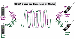
CDMA- Each pair should communicate in different languages. What is the advantage here? We are not waiting for others, ie, there is no waste of time. We can speak in the same pitch, since the language is different.

FDMA, TDMA, CDMA Analogy


In TDMA(Time Division Multiple Access),the bandwidth is just one channel that is timeshared between different stations.Each station is allocated a time slot during which it can send data and each station transmits its data in is assigned time slot.


In CDMA(Code Division Multiple Access),one channel carries all transmissions simultaneously and using a unique code for each transmitted signal,the mobile and base station are able to distinguish between signals transmitted simultaneously over the same freuqency allocation.


In FDMA(Frequency Division Multiple Access),the available bandwidth of the common channel is divided into bands that are separated by guard bands(to prevent station interferences).Each staion is allocated a band to send its data and also uses a bandpass filter to confine the transmitter frequencies.

FDMA Bandwidth slicing


Operation of MEMS Bistable Switch

MEMS:

Microelectromechanical systems (MEMS) also referred to as micromachines (in Japan), or micro systems technologyMST (in Europe).MEMS are separate and distinct from the hypothetical vision of molecular nanotechnology or molecular electronics. MEMS are made up of components between 1 to 100 micrometres in size (i.e. 0.001 to 0.1 mm), and MEMS devices generally range in size from 20 micrometres (20 millionths of a metre) to a millimetre (i.e. 0.02 to 1.0 mm). They usually consist of a central unit that processes data (the microprocessor) and several components that interact with the outside such as microsensors.

Working:

The animation shows the bistable switch moving from the "off" position to the "on" position. The transition from "on" to "off" involves an identical set of operations.
The device operates in two dimensions, so it is easily implemented in MEMS by the MUMPS process. Certain parts of the structure became POLY1 and certain parts became POLY2, but the operation is identical to that shown here.


Operation of the Switch:
  1. The purple platform is independently disengaged from the wheel.
  2. The dark blue rod is pulled to signal a toggle.
  3. The red lever structure amplifies the input movement.
  4. The green arm advances the orange ratchet wheel one position, rotating around the yellow hub.
  5. The green arm flicks back over the tooth so it can work again.
  6. The light blue pawl holds the wheel while the green arm resets.
  7. The purple platform engages again.
  8. The new resting position of the platform is now different. 


Hardwork Can Never Ever Fails...
Best Luck...

Digital Clock-Working Animation

How it works?


Each clock requires an oscillator.For a digital clock, this is generally provided by a crystal. The crystal is made from glass. When an electric charge is sent through the crystal it changes shape very slightly and creates a very slight sound. The sound is at a regular frequency which is converted to an electronic signal. The oscillations of a 60 Hertz oscillator can then be reduced to a 1 Hertz oscillation by a series of counters, the first counts one every ten oscillations and the second counts one every six counts of the 10 counter. The 1 Hertz signal is now perfectly set up to indicate the passing of seconds, because the definition of 1 Hertz is one oscillation per second!


The 1 Hertz oscillation is further reduced by a 10 counter in order to figure the minutes and another 6 counter added after that will give the number of hours. Each counter is then connected to a chip that converts the count on the counter to a signal to a "7-segment" display, to indicate the number counted for that particular counter. A "7-segment display" is a very familiar device that is seen on the face of most digital clocks. It can be an LED (light emitting diode) or an LCD (liquid crystal display).


When a digital clock clicks over from 12:59 to 1:00 it has to be reset to, in effect, start over. Most digital clocks will be equipped with a built in processor looking for the number 13 in the hours column and when this occurs sets the hour counter back to 1. For a user to set the clock to the correct time, buttons are installed that allow increased frequencies to flow through the minute or hour counters, causing them to move faster. 


Hardwork Can Never Ever Fails...
Best Luck... 

BI-CMOS Inverter-working

BICMOS:


Two bipolar transistors (T3 and T4), one nMOS and one pMOS transistor (both enhancement-type devices, OFF at Vin=0V)
The MOS switches perform the logic function & bipolar transistors drive output loads

Vin = 0 

--T1 is off.   Therefore T3 is non-conducting
--T2 ON - supplies current to base of T4
--T4 base voltage set to Vdd.
--T4 conducts & acts as current source to charge load CL towards Vdd.
--Vout rises to Vdd - Vbe (of T4) 
  Note :          Vbe (of T4) is base-emitter voltage of  T4.
 (pullup bipolar transistor turns off as the output approaches
 5V - Vbe (of T4))
                       
  Vin = Vdd 

--T2 is off. Therefore T4 is non-conducting.
--T1 is on and supplies current to the base of T3
--T3 conducts & acts as a current sink to discharge load CL towards 0V.
--Vout falls to 0V+ VCEsat (of T3) 
Note : VCEsat (of T3) is saturation V from T3 collector to emitter 

T3 & T4 present low impedances when turned on into saturation & load CL will be
  charged or discharged rapidly
          Output logic levels will be good & will be close to rail voltages since VCEsat  is quite
   small & VBE » 0.7V. Therefore, inverter has high noise margins 
          Inverter has high input impedance, i.e., MOS gate input
          Inverter has low output impedance
          Inverter has high drive capability but occupies a relatively small area
          However, this is not a good arrangement to implement since no discharge path
   exists for current from the base of either bipolar transistor when it is being turned
   off, i.e.,  
                     when Vin=Vdd, T2 is off and no
                conducting path to the base of T4 exists  
                    when Vin=0,      T1 is off and
                                         no conducting path to the base of T3 exists
   This will slow down the action of the circuit


Hardwork Can Never Ever Fails..
Best Luck...


Photoresistor

A Photoresistor or Light Dependent Resistor (LDR) is a resistor whose resistance decreases with increasing incident light intensity; in other words, it exhibits photoconductivity.
A Photoresistor is made of a high resistance semiconductor. If light falling on the device is of high enough frequency, photons absorbed by the semiconductor give bound electrons enough energy to jump into the conduction band. The resulting free electron (and its hole partner) conduct electricity, thereby lowering resistance.
A Photoelectric device can be either intrinsic or extrinsic. An intrinsic semiconductor has its own charge carriers and is not an efficient semiconductor, e.g. silicon. In intrinsic devices the only available electrons are in the valence band, and hence the photon must have enough energy to excite the electron across the entire bandgap. Extrinsic devices have impurities, also called dopants, added whose ground state energy is closer to the conduction band; since the electrons do not have as far to jump, lower energy photons (i.e., longer wavelengths and lower frequencies) are sufficient to trigger the device. If a sample of silicon has some of its atoms replaced by phosphorus atoms (impurities), there will be extra electrons available for conduction. This is an example of an extrinsic semiconductor. Photoresistors are basically photocells.
Fig 1 Symbol of photo resistor


Fig 2 Photo resistor
 

Wednesday, August 01, 2012

Ultra Capacitor

It is a charge storing device but different in construction with respect to normal capacitor.Capacitance range upto 5000F.Also called double layered
--No chemical reactions involved.
--Works at -40 degree celsius.
--It stores 5% more energy than lithium ion battery.
--Much more effective at rapid, regenerative energy storage than chemical batteries.

Inside a super capacitor:

Working:

--When a voltage is applied,the ions are attracted to the electrode with the opposite charge,where they cling electrostatically to the pores of the carbon
-- At low voltages used in ultracapacitors, carbon is inert and does not react chemically with the ions attached to it.Nor the ions become ionized or reduced,as they do at the higher voltages used in an electrolytic cell.
--As the effective area where ions are stuck is much larger,appreciably high value of capacitance is obtained.


Hardwork Can Never Ever Fails...
Best Luck...


How pendrive Works?

Pendrive:

A printed circuit board carrying the circuit elements and a USB connector is shown in the above image. The circuitry is protected inside a pair of plastic cases (connected to each other by means of mechanical hooks) which can be carried in a pocket or a key chain. The USB connector is protected by either retracting into the body or by covering by a removable lid. There are two chips, one is the USB controller and the other is the flash memory chip.
 
The IC SK6211 shown in the above image is a controller which facilitates the data communication between the PC/Laptop and the flash memory (EEPROM) of the pen drive. It is fully compatible with USB 2.0 protocols and USB Mass storage class V1.0 specification. The devices like memory card, hard disk, pen drive etc with high data storage capacity fall under the category of Mass Storage Devices. In order to communicate data with devices falling under this category the USB has defined a set of protocols. The operating system provides inbuilt libraries to handle such devices thereby preventing the need of any external drivers to be installed before using these devices. This controller IC can interface with all kind of NAND EEPROM.
The second chip which is shown in the image above is a NAND type flash memory which has fast read, write and erase cycles. The data is stored in memory cells of the EEPROM, known as “floating gate transistors” - a regular metal-oxide field effect transistor (M0SFET) consisting three terminals - source, gate and drain. The storage capacity of this memory is 2GB. There is another similar chip with storage capacity of 2GB on the other side of the PCB, thereby making the total capacity of the pen drive to be 4GB. 

The above image shows the other side of PCB. The second memory chip, a crystal oscillator and a number of surface mount components are soldered which are required for the operation of the pen drive.
The crystal oscillator produces the clock signal for the correct operation of the device. The crystal oscillator used here runs at a clock frequency at 12 MHz.


Hardwork Can Never  Ever Fails..
Best Luck...


How LED producing different colours?

LED working


The P type semiconductor is connected with the positive end of battery and N type with the negative end of the battery. When a current is passed through the LED, free electrons from the N layer moves to the P layer in the active region (P-N Junction). This involves a drop from the conduction band to the lower orbit and electrons release some energy in the form of photons. The frequency and wavelength of the light produced photons is dependent on the material and doping level of the semiconductor. In case of LED, the material used and doping levels are set so as to produce photons with wavelength in the range of desired color of light in the visible spectrum.


Light Emitting Diodes are made from exotic semiconductor compounds such as Gallium Arsenide (GaAs), Gallium Phosphide (GaP), Gallium Arsenide Phosphide (GaAsP), Silicon Carbide (SiC) or Gallium Indium Nitride (GaInN) all mixed together at different ratios to produce a distinct wavelength of colour. Different LED compounds emit light in specific regions of the visible light spectrum and therefore produce different intensity levels. The exact choice of the semiconductor material used will determine the overall wavelength of the photon light emissions and therefore the resulting colour of the light emitted.


How to calculate the value of the Series Resistor for an LED?


How 3 Phase Power Supply works?

3 Phase current flow


In a three-phase system, three circuit conductors carry three alternating currents (of the same frequency) which reach their instantaneous peak values at different times. Taking one conductor as the reference, the other two currents are delayed in time by one-third and two-thirds of one cycle of the electric current. This delay between phases has the effect of giving constant power transfer over each cycle of the current and also makes it possible to produce a rotating magnetic field in an electric motor.

What is an Adhoc Network?

Characteristics of Ad Hoc Network


An ad hoc network is a collection of information technology devices such as PDAs or sensors, which can form a communications network without the need for a wireless communication interface. Due to the limited range of each device's wireless transmission, a device can forward information via other devices to its desired destination.

Illustration of an Ad-Hoc Network

Animated Electronics


A good collection of Electronics animations in Java applet is available in the following Blog.

Please CLICK HERE to visit the Blog.

I think it will be useful for all...


How Yagi-Uda antenna works?

Yagi antenna, also known as a Yagi-Uda array or simply a Yagi, is a unidirectional antenna commonly used in communications when a frequency is above 10 MHz. It is used at some surface installations in satellite communications systems.

A basic Yagi consists of two or three straight elements, each measuring approximately1/2 electrical wavelengths. The antenna can be balanced or unbalanced. The Yagi is inherently a balanced antenna, but it can be fed with coaxial cable and a device called a balunat the point where the feed line joins the driven element.

The driven element of a Yagi is the equivalent of a center-fed, half-wave dipole antenna. Parallel to the driven element, and approximately 0.2 to 0.5 wavelength on either side of it, are straight rods or wires called reflectors and directors. A reflector is placed behind the driven element and is slightly longer than 1/2 wavelength; a director is placed in front of the driven element and is slightly shorter than 1/2 wavelength. A typical Yagi has one reflector and one or more directors. The antenna propagates electromagnetic field energy in the direction running from the driven element toward the director(s), and is most sensitive to incoming electromagnetic field energy in this same direction.
The Yagi antenna not only has a unidirectional radiation and response pattern, but it concentrates the radiation and response. The more directors a Yagi has, the greater the so-called forward gain. As more directors are added to a Yagi, it becomes longer. Some Yagi antennas have as many as 10 or even 12 directors in addition to the driven element and one reflector. Long Yagis are rarely used below 50 MHz, because at these frequencies the structure becomes physically unwieldy.
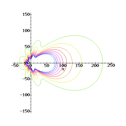
 Radiation pattern of Yagi-Uda antenna


Animation of radiation pattern of Yagi-Uda antenna