Showing posts with label Digital Electronics. Show all posts
Showing posts with label Digital Electronics. Show all posts
Thursday, July 16, 2015


Thursday, February 14, 2013
An Introduction to Digital Logic Families
What is a Logic Family?
In Digital Designs, our primary aim is to create an Integrated Circuit (IC).
In Digital Designs, our primary aim is to create an Integrated Circuit (IC).
A Circuit configuration or arrangement of the circuit elements in a special manner will result in a particular Logic Family.
What are the advantages of creating different Logic Families?
Electrical Characteristics of the IC will be identical. In other words, the different parameters like Noise Margin, Fan In, Fan Out etc will be identical.
Different ICs belonging to the same logic families will be compatible with each other.
Some Characteristics we consider for the selection of a particular Logic Family are:
- Supply voltage range
- Speed of response
- Power dissipation
- Input and output logic levels
- Current sourcing and sinking capability
- Fan-out
- Noise margin
The basic Classification of the Logic Families are as follows:
- Bipolar Devices
- MOS Devices
- Hybrid Devices
- Diode Logic (DL)
- Resistor Transistor Logic (RTL)
- Diode Transistor Logic (DTL)
- Transistor- Transistor Logic (TTL)
- Emitter Coupled Logic (ECL) or Current Mode Logic (CML)
- Integrated Injection Logic (IIL)
- P-MOS Family
- N-MOS Family
- Complementary-MOS Family
- Standard C-MOS
- Clocked C-MOS
- Bi-CMOS
- Pseudo N-MOS
- C-MOS Domino Logic
- Pass Transistor Logic
- Bi-CMOS Family
In DL (diode logic), only Diode and Resistors are used for implementing a particular Logic.Remember that the Diode conducts only when it is Forward Biased.
Disadvantages of Diode Logic
- Diode Logic suffers from voltage degradation from one stage to the next.
- Diode Logic only permits OR and AND functions.
In RTL (resistor transistor logic), all the logic are implemented using resistors and transistors. One basic thing about the transistor (NPN), is that HIGH at input causes output to be LOW (i.e. like a inverter). In the case of PNP transistor, the LOW at input causes output to be HIGH.
 |
| RTL Circuit |
- Less number of Transistors
Disadvantage:
- High Power Dissipation
- Low Fan In
In DTL (Diode transistor logic), all the logic is implemented using diodes and transistors.
 |
| DTL Logic |
- Propagation Delay is Larger
In Transistor Transistor logic or just TTL, logic gates are built only around transistors.
TTL Logic has the following sub-families:
- Standard TTL.
- High Speed TTL
- Low Power TTL.
- Schhottky TTL.
- Low Power Schottky TTL
- Advanced Schottky TTL
- Advanced Low Power Schottky TTL
- Fast Schottky
The main specialty of ECL is that it is operating in Active Region than the Saturation Region. That is the reason for its high speed operation. As you can see in the figure, the Emitters of the Transistors Q1 and Q2 are coupled together.
 |
| Emitter Coupled Pair |
Disadvantage:
- Large Silicon Area
- Large Power Consumption
Thursday, November 22, 2012
Clock Skew and jitter in digital
Jitter is nothing but the displacement of signal from its original position.This movement may lag or lead from its original or ideal position.As a speed increases, the edge deviation cause a significant problems like signal integrity,skew,race condition and other timing problems.


Classification
1. cycle-to-cycle jitter
Cycle-to-cycle jitter is the change in an output’s transition in time in relation to the transition during the previous cycle.
2.period jitter
Period jitter is the maximum change in a signal transition from the ideal position in time. Phase jitter, also called long-term jitter, in the maximum change in an output signal transition from its ideal position over many cycles (typically 10 to 20 microseconds).
3.phase jitter
Phase jitter may leads to the displacement of phase from one signal to another.
Figure A: cycle to cycle jitter

skew
Skew deals with the propagation delay of the output signal.It is the variation of propagation delay differences between output signals.Excessive skew, especially for clock signals, can cause race conditions and other timing errors that result in system data faults. At the very least, poor skew will force a slower maximum system speed, and this, in turn, will limit system performance.
Hardwork Can Never Ever Fails...
Best Luck....
Saturday, November 10, 2012
Propogation Delay and Glitch
Propogation Delay:
Propagation delay is a time associated with any digital circuit and is the time between when an input to the circuit changes until that change propagates through the circuit and changes the output. Every digital gate (And, Or, Inverter,...) has its own propagation delay. For single gates this delay can be very short, maybe somewhere around nano seconds or shorter. But as the circuit grows larger and more components are put one after another, the delay increases too. Figure below shows the propagation delay effect of a simple inverter on its output where Tp is the propagation time:

In a more complex circuit every input can go through many different paths until it reaches the output. Every path in the circuit also has a different delay and for a single input, the propagation delay is the delay of the path with the longest delay because it takes that much time for that input to give a valid output. For a multiple input circuit, the propagation delay is equal to the maximum delay in the circuit. This is because if the output of the circuit is read shorter than the maximum delay, in some cases the output might not be valid and can result in false interpretations and actions.


The difference in propagation delay of different circuit paths can result in glitches on the output.
Glitch:
A glitch is called to an invalid and unpredicted output of a digital circuit that can be read by the next stage and result in a wrong action. Glitches happen mostly due to propagtion delays in a digital circuit. For example assume a circuit as below:
When input I=1, the output is 1 as one of the inputs to the OR gate is one. When I=0 also the output is 1 as the output of the inverter will be 1 going to the OR gate. So for both these cases the output should remain as 1. But let's see what happens when we assume some propagation delay for the inverter. Below you can see the signals to the circuit and the output:

You can see that when the input change from 1 to 0, it takes a short time for the inverter to provide a 1 at its output due to its propagation delay. Therefore for that short period of time both inputs to the OR gate are zero, resulting in a zero at the output of the OR gate. Then finally after the inverter output changes to 1, the OR gates output changes to one too.
This example shows happening of an unexpected zero ar the circuit. This is a glitch and can cause problem for the rest of the circuit as it will propagate into the next circuits and result in more and more glitches.
Ways to avoid glitch:
There are ways to avoid such glitches. One of the most practical ways is to put a timed gate such as a latch or a flip-flop to isolate the output of this circuit from the next circuit and allow the output to the next circuit only when it is valid and there are no glitches. The digital signal that allows the output of this circuit to pass through must wait for enough time since the inputs change until all the glitches pass, which would be more than the maximum propagation delay of the circuit. Then it can let the output of the circuit to be presented to the next stage.
The propagation delay of a circuit is an important factor on how fast the circuit can work. When one block of the circuit has a high delay, all the rest of the circuit will have to wait for this one block to provide a valid output.
Hardwork Can Never Ever Fails...
Best Luck...
Tuesday, October 09, 2012
Why all Digital Electronics Circuits use DC and Not AC?
The question will be little confusing.
But the answer is simple.
In Digital Electronics, Gates are the basic Elements.
Actually this Gates are made up of Transistors.
Transistors are working as a Switch in Digital Electronics.
ie, When control signal is present, Transistor is ON, otherwise Transistor is OFF.
Now, What is this Control Signal?
That is the Signal Applied to the Base of the Transistor.
The Switch must be ON till the control signal is present and the Switch must be OFF till the control signal is absent.
Now consider applying AC signal as the control signal to the Base of the Transistor.
The AC signal will vary from Positive peak to Negative peak going through the 0V.
So how can we keep the Transistor ON and OFF as per our requirement?
It is not possible.
Now consider DC. It is Direct current and it is constant in value.
So if we apply DC to the Base of the Transistor as a control signal, we can keep the Transistor ON of OFF as per our wish.
That is In digital Electronics, We need only HIGH signal and LOW signal, not the intermediate values.
Hence we cannot use AC in Digital.
Now consider Transistor working as an AMPLIFIER.
Here also, the transistor is working in DC (Power supply of the Transistor is DC), but the input is an AC signal.
Thus Amplification of AC signal is just an application of the Transistor and that doesn't mean that the Transistor is working in AC.
Why cant we power the Transistor with AC?
We can apply AC as a Power supply to the Transistor.
But the transistor will not give the desired operation.
Because, for acting as a Switch or Amplifier, the transistor should be biased.
In order to keep the transistor in constant Biasing conditions, we need Constant current. ie DC.
If we apply AC as a power supply to the transistor, the Biasing conditions of the Transistor will be varying in each cycle of the AC signal.
Hence the transistor will not work properly.
This is the reason why we convert the AC signals into DC using Rectifiers in the Power supply section of the Electronic Devices.
(We can apply the same principle to MOSFET also.
MOSFET are used as switches in Digital Electronics as Switches.
Working principle of MOSFET is same as that of the Transistor.
However, MOSFET is a Voltage controlled Device, but Transistor is a Current controlled Device.)
But the answer is simple.
 |
| AC Vs DC |
In Digital Electronics, Gates are the basic Elements.
Actually this Gates are made up of Transistors.
 |
| NAND gate using Transistors |
Transistors are working as a Switch in Digital Electronics.
 |
| Transistor as a Switch |
ie, When control signal is present, Transistor is ON, otherwise Transistor is OFF.
Now, What is this Control Signal?
That is the Signal Applied to the Base of the Transistor.
The Switch must be ON till the control signal is present and the Switch must be OFF till the control signal is absent.
 |
| Switch with Control Terminal |
Now consider applying AC signal as the control signal to the Base of the Transistor.
The AC signal will vary from Positive peak to Negative peak going through the 0V.
So how can we keep the Transistor ON and OFF as per our requirement?
It is not possible.
Now consider DC. It is Direct current and it is constant in value.
So if we apply DC to the Base of the Transistor as a control signal, we can keep the Transistor ON of OFF as per our wish.
That is In digital Electronics, We need only HIGH signal and LOW signal, not the intermediate values.
Hence we cannot use AC in Digital.
Now consider Transistor working as an AMPLIFIER.
Here also, the transistor is working in DC (Power supply of the Transistor is DC), but the input is an AC signal.
 |
| Transistor as an Amplifier |
Thus Amplification of AC signal is just an application of the Transistor and that doesn't mean that the Transistor is working in AC.
Why cant we power the Transistor with AC?
We can apply AC as a Power supply to the Transistor.
But the transistor will not give the desired operation.
 |
| Biasing of Transistor (a) NPN (b) PNP |
Because, for acting as a Switch or Amplifier, the transistor should be biased.
In order to keep the transistor in constant Biasing conditions, we need Constant current. ie DC.
If we apply AC as a power supply to the transistor, the Biasing conditions of the Transistor will be varying in each cycle of the AC signal.
Hence the transistor will not work properly.
This is the reason why we convert the AC signals into DC using Rectifiers in the Power supply section of the Electronic Devices.
(We can apply the same principle to MOSFET also.
MOSFET are used as switches in Digital Electronics as Switches.
Working principle of MOSFET is same as that of the Transistor.
However, MOSFET is a Voltage controlled Device, but Transistor is a Current controlled Device.)
Thursday, August 30, 2012
Binary to Gray Code Converter
Gray code equivalent of the given binary number is computed as follows:
g3 = b3
g2 = b3 ⊕ b2
g1 = b2 ⊕ b1
g0 = b1 ⊕ b0
g2 = b3 ⊕ b2
g1 = b2 ⊕ b1
g0 = b1 ⊕ b0
A binary to gray code converter can be implemented using XOR gates. For n input, n-1 gates are required. As shown in the image below for 4 inputs, 3 XOR gates are used:
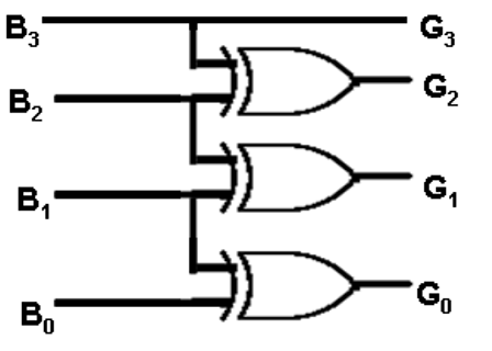
CONVERTING BETWEEN GRAY AND BINARY CODES ANIMATION
Gray to Binary Code Converter
Binary code equivalent of the given gray number is computed as follows:b3 = g3b2 = b3 ⊕ g2b1 = b2 ⊕ g1b0 = b1 ⊕ g0A gray to binary code converter can be implemented using XOR gates. For n input, n-1 gates are required. As shown in the image below for 4 inputs, 3 XOR gates are used:

Wednesday, August 08, 2012
All about FLIP FLOPS - Animation
I have gone through a fantastic Flash Animation of Flip Flops.
I got a clear idea about the difference between LATCH and FLIP FLOP through this animation.
You can learn all the basics of Flip Flops here.
Please CLICK HERE to view the animations
 |
| Difference between LATCH and FLIP FLOP |
I got a clear idea about the difference between LATCH and FLIP FLOP through this animation.
You can learn all the basics of Flip Flops here.
Please CLICK HERE to view the animations
Monday, August 06, 2012
Shift Register
A register is a semiconductor device that is used for storing several bits of digital data. It basically consists of a set of flip-flops, with each flip-flop representing one bit of the register.
Thus, an n-bit register has n flip-flops.
A basic register is also known as a 'latch.'
A special type of register, known as the shift register, is used to pass or transfer bits of data from one flip-flop to another.
This process of transferring data bits from one flip-flop to the next is known as 'shifting'.
Shift registers are useful for transferring data in a serial manner while allowing parallel access to the data.
A shift register is simply a set of flip-flops interconnected in such a way that the input to a flip-flop is the output of the one before it.
Clocking all the flip-flops at the same time will cause the bits of data to shift or move to the right in one direction (i.e., toward the last flip-flop) .
Figure shows a simple implementation of a 4-bit shift register using D-type flip-flops.
Under its basic operation, the data bit of the last flip-flop is lost once it is clocked out.
In some applications there is a need to bring this back to the first flip-flop, in which case the data will just be circulated within the shift register. A shift register connected this way is known as an end-around-carry shift register, or simply 'ring counter'.
A more complicated version of a shift register is one that allows shifting in both directions, left or right.
It is aptly and quite descriptively referred to as the Shift-Right Shift-Left Register.
To accomplish this, a 'Mode' control line is added to the circuit. The state of this 'Mode' input determines whether the shift direction would be right or left.
Thus, an n-bit register has n flip-flops.
A basic register is also known as a 'latch.'
A special type of register, known as the shift register, is used to pass or transfer bits of data from one flip-flop to another.
This process of transferring data bits from one flip-flop to the next is known as 'shifting'.
 |
| Basic Idea of Shift Register |
Shift registers are useful for transferring data in a serial manner while allowing parallel access to the data.
A shift register is simply a set of flip-flops interconnected in such a way that the input to a flip-flop is the output of the one before it.
Clocking all the flip-flops at the same time will cause the bits of data to shift or move to the right in one direction (i.e., toward the last flip-flop) .
Figure shows a simple implementation of a 4-bit shift register using D-type flip-flops.
 |
| A Simple Shift Register Consisting of D-type Flip-flops |
In some applications there is a need to bring this back to the first flip-flop, in which case the data will just be circulated within the shift register. A shift register connected this way is known as an end-around-carry shift register, or simply 'ring counter'.
 |
| Parallel In Serial Out Shift Register |
A more complicated version of a shift register is one that allows shifting in both directions, left or right.
It is aptly and quite descriptively referred to as the Shift-Right Shift-Left Register.
To accomplish this, a 'Mode' control line is added to the circuit. The state of this 'Mode' input determines whether the shift direction would be right or left.
Saturday, August 04, 2012
Sequential Logic Circuits
Unlike Combinational Logic
circuits that change state depending upon the actual signals being applied to their inputs at that time, Sequential Logic
circuits have some form of inherent "Memory" built in to them as they are able to take into account their previous input
state as well as those actually present, a sort of "before" and "after" is involved with sequential circuits.
In other words, the output state of a sequential logic circuit is a function of the following three states, the
"present input", the "past input" and/or the "past output". Sequential Logic circuits remember these conditions and stay
fixed in their current state until the next clock signal changes one of the states, giving sequential logic circuits "Memory".
Sequential logic circuits are generally termed as two state or
Bistable
devices which can have their output
or outputs set in one of two basic states, a logic level "1" or a logic
level "0" and will remain "latched" (hence the name latch)
indefinitely in this current state or condition until some other input
trigger pulse or signal is applied which will cause the bistable
to change its state once again.
Sequential Logic Representation

The word "Sequential" means that things happen in a "sequence", one after another and in
Sequential Logic circuits, the actual clock signal determines when things will happen next. Simple
sequential logic circuits can be constructed from standard Bistable circuits such as Flip-flops,
Latches and Counters and which themselves can be made by simply
connecting together universal NAND Gates
and/or NOR Gates in a particular
combinational way to produce the required sequential circuit.
Classification of Sequential Logic
As standard logic gates are the building blocks of combinational circuits, bistable latches and flip-flops
are the building blocks of Sequential Logic Circuits.
Sequential logic circuits can be constructed
to produce either simple edge-triggered flip-flops or more complex
sequential circuits such as storage registers, shift registers,
memory devices or counters. Either way sequential logic circuits can be
divided into the following three main categories:
- 1. Event Driven - asynchronous circuits that change state immediately when enabled.
- 2. Clock Driven - synchronous circuits that are synchronized to a specific clock signal.
- 3. Pulse Driven - which is a combination of the two that responds to triggering pulses.

Friday, August 03, 2012
Binary decoder
A decoder is a multiple-input, multiple-output logic circuit that converts coded inputs into coded outputs, where the input and output codes are different; e.g. n-to-2n, BCD decoders. Enable inputs must be on for the decoder to function, otherwise its outputs assume a single "disabled" output code word.Decoding is necessary in applications such as data multiplexing, 7 segment display and memory address decoding. Figure below shows the pseudo block of a decoder.
.gif) Basic Binary Decoder AND gate can be used as the basic decoding element, because its output is HIGH only when all its inputs are HIGH. For example, if the input binary number is 0110, then, to make all the inputs to the AND gate HIGH, the two outer bits must be inverted using two inverters as shown in figure below.
| ||||||||||||||||||||||||||||||||


Subscribe to:
Posts (Atom)