The python implementation, mathematical background, and noise removal using Fourier Transform are explored in this VIDEO..
Showing posts with label Electronic Devices. Show all posts
Showing posts with label Electronic Devices. Show all posts
Sunday, May 16, 2021


Thursday, July 16, 2015
Wednesday, December 24, 2014
How Mosquito Racket works?
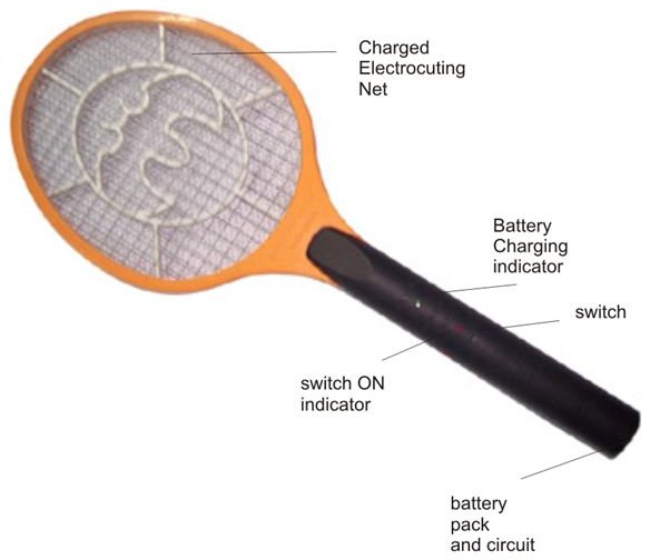
Parts:
1. Power Supply
2. Oscillator
3. Transformer(Step-up)
4, Final mesh-nets
The circuit consists of a flyback topology transformer driven by a general NPN transistor 2SD965.
The feedback coil of transformer is of 10 turns, the primary is of 40 turns and the output or secondary coil is of 450 turns (40:450).
When this circuit is run by giving input of 3 Volts, the transformer generates about 2000-4000 volts at zero load, and the output is then coupled 3 times by using three IN4007 diodes and suitable capacitors, thus reaching our need of 5000-10,000 volts.

The moment a mosquito or any bug comes in contact with the meshes, the stored high voltage in the capacitor discharges violently through the body of the entangled bug creating a big spark and electrocuting it instantly.
Monday, October 21, 2013
Why Silicon is preferred over Germanium for Semiconductor Devices?
As we all know, both Silicon and Germanium are semiconductor devices. But the present trend is to use Silicon instead of Germanium. What may be the reasons?
 |
- At room temperature, Silicon crystal has fewer free electrons than Germanium crystal. This implies that silicon will have much smaller Collector cut off current than Germanium.
- The variation of Collector cut off current with temperature is less in Silicon compared to Germanium.
- The structure of Germanium crystals will be destroyed at higher temperature. However, Silicon crystals are not easily damaged by excess heat.
- Peak Inverse Voltage ratings of Silicon diodes are greater than Germanium diodes.
- Si is less expensive due to the greater abundance of element. The major raw material for Si wafer fabrication is sand and there is lots of sand available in nature.
But there is a disadvantage for Silicon over Germanium.
The potential Barrier of Silicon is more compared to Germanium.
But if we consider the advantages listed above, we can conclude that Silicon is the best element for the Semiconductor Devices and Applications.
However, the first transistor was made of germanium (Ge). :)
Sunday, March 17, 2013
MAGNETIC RESONANCE IMAGING
Magnetic Resonance Imaging (MRI), nuclear magnetic resonance imaging (NMRI), or magnetic resonance tomography (MRT) is a medical imaging technique used in radiology to visualize internal structures of the body in detail. MRI makes use of the property of nuclear magnetic resonance (NMR) to image nuclei of atoms inside the body.
An MRI scanner is a device in which the patient lies within a large, powerful magnet where the magnetic field is used to align the magnetization of some atomic nuclei in the body, and radio frequency magnetic fields are applied to systematically alter the alignment of this magnetization. This causes the nuclei to produce a rotating magnetic field detectable by the scanner—and this information is recorded to construct an image of the scanned area of the body. Magnetic field gradients cause nuclei at different locations to precess at different speeds, which allows spatial information to be recovered using Fourier analysis of the measured signal. By using gradients in different directions, 2D images or 3D volumes can be obtained in any arbitrary orientation.
MRI provides good contrast between the different soft tissues of the body, which makes it especially useful in imaging the brain, muscles, the heart, and cancers compared with other medical imaging techniques such ascomputed tomography (CT) or X-rays. Unlike CT scans or traditional X-rays, MRI does not use ionizing radiation.
How MRI works
MRI machines make use of the fact that body tissue contains lots of water, and hence protons which get aligned in a large magnetic field. Each water molecule has two hydrogen nuclei or protons. When a person is inside the powerful magnetic field of the scanner, the average magnetic moment of many protons becomes aligned with the direction of the field. A radio frequency current is briefly turned on, producing a varying electromagnetic field. This electromagnetic field has just the right frequency, known as the resonance frequency, to be absorbed and flip the spin of the protons in the magnetic field. After the electromagnetic field is turned off, the spins of the protons return to thermodynamic equilibrium and the bulk magnetization becomes re-aligned with the static magnetic field. During this relaxation, a radio frequency signal is generated, which can be measured with receiver coils.
Information about the origin of the signal in 3D space can be learned by applying additional magnetic fields during the scan. These additional magnetic fields can be used to only generate detectable signal from specific locations in the body (spatial excitation) and/or to make magnetization at different spatial locations precess at different frequencies, which enables k-space encoding of spatial information. The 3D images obtained in MRI can be rotated along arbitrary orientations and manipulated by the doctor to be better able to detect tiny changes of structures within the body. These fields, generated by passing electric currents through gradient coils, make the magnetic field strength vary depending on the position within the magnet. Because this makes the frequency of the released radio signal also dependent on its origin in a predictable manner, the distribution of protons in the body can be mathematically recovered from the signal, typically by the use of the inverse Fourier transform.
Protons in different tissues return to their equilibrium state at different relaxation rates. Different tissue variables, including spin density, T1 and T2 relaxation times, and flow and spectral shifts can be used to construct images. By changing the settings on the scanner, this effect is used to create contrast between different types of body tissue or between other properties, as in fMRI and diffusion MRI.

MRI is used to image every part of the body, and is particularly useful for tissues with many hydrogen nuclei and little density contrast, such as the brain, muscle, connective tissue and most tumors.
Thursday, February 14, 2013
What is Darlington Pair?
This is two transistors connected together so that the amplified current from the first is amplified further by the second transistor.

This gives the Darlington pair a very high current gain such as 10000.
Darlington pairs are sold as complete packages containing the two transistors.
They have three leads (B, C and E) which are equivalent to the leads of a standard individual transistor.
This gives the Darlington pair a very high current gain such as 10000.
Darlington pairs are sold as complete packages containing the two transistors.
They have three leads (B, C and E) which are equivalent to the leads of a standard individual transistor.
CMOS Vs TTL
The difference between the two Logic Styles are:
Since TTL has very little parasitic capacitance, the time delay is very small, & TTL is faster.
MOSFETs, based on voltage operations, have much greater capacitances, the charging & discharging of which consumes time (Ref: RC time constant), hence CMOS is slower.
- TTL circuits utilize BJTs while CMOS circuits utilize FETs.
- CMOS allows a much higher density of logic functions in a single chip compared to TTL.
- TTL circuits consumes more power compared to CMOS circuits at rest.
- CMOS chips are a lot more susceptible to static discharge compared to TTL chips
- Propagation delay is more in CMOS compared to TTL
- Switching Speed is More for TTL compared to CMOS.
- CMOS devices are cheaper than TTL Devices.
- The Power Supply requirement for TTL is 3 to 15V, small fluctuations are tolerated.
- The Power Supply requirement for CMOS is 5V ±0.25V, it must be very smooth, a regulated supply.
- TTL Can handle only less frequency compared to CMOS.
Since TTL has very little parasitic capacitance, the time delay is very small, & TTL is faster.
MOSFETs, based on voltage operations, have much greater capacitances, the charging & discharging of which consumes time (Ref: RC time constant), hence CMOS is slower.
Saturday, February 09, 2013
Short Notes on Bipolar transistors
NPN Transistor
Placing P-type semiconductor between two N-type semiconductor is NPN transistor

It operates by a small current flow from the emitter to base.current will not flow from the emitter to the collector until a small voltage (at least 0.7 volts) is applied to the base.

Collector current is much larger than the base current.
SYMBOL

PNP Transistor
Placing N-type semiconductor between two P-type semiconductor is PNP transistor.

Its operation is same as NPN but reversed.The voltage relations also reversed.So to turn on the device both the collector and base must be negative.

PNP symbol

Amplification:
Transistors are used as amplifiers to increase the input signals in TV ,stereo and others applications.It is often called as linear electronics since it contains direct relation with the input and output signal.

If the base is given with the power,it gets biased.It switch on the transistor.An increase or decrease in the input signals makes an increase and decrease in the output signal but with the signal inverse.Frequency remains the same.
Gain:
The measure of amplification is the gain.
For example, if
the input signal has an amplitude of 0.2 volts, and the output signal
has an amplitude of 10 volts, then:

Power gain =current gain x voltage gain.
Switching
Transistors can also be used for switching in case of digital circuits.Digital circuits needs switch on and off.


When the base voltage is about 0.85 volts, sufficient base current flows to turn the transistor fully on. The collector voltage drops to approximately half a volt because of the voltage drop across the collector resistor. A transistor which is conducting the maximum current is said to be in saturation.
Transistor Application
Linear:
Amplifiers
Digital:
Computers
Courtesy:http://silver-fox.ca
Hardwork Can Never Ever Fails..
Best Luck..
Friday, February 08, 2013
3D View of PN Junction
 | |||
| P Type and N Type Materials- Before forming the Junction |
 |
| P and N type Materials Brought together |
 |
| Recombination Started (Gold Balls- Recombination) |
 |
| Depletion Region Formed |
(From the article: 'Education in Three Dimensions: Using Virtual Reality in Education for Illustrating Spatial Relationships' by ALLPORT, Christopher, SINES, Paul, SCHREINER, Brandon & DAS, Biswajit)
Sunday, February 03, 2013
How Electric fan work
An electric fan is an electric motor with some fan blades attached to its rotating shaft. As the motor spins, the fan blades rotate. Each blade is angled a bit, and as the inclined plane of the blade moves through the air, it forces the air ahead of it forward. Each blade does this on a continuous basis, and the result is a moving air stream. The fan is taking air from the area behind itself and blowing it out the front. The fan generates a movement of air, causing the warm, less dense air to rise, and the cool, dense air to descend, thus creating a feeling of coolness in the air.

Wednesday, January 30, 2013
HOW METAL DETECTOR WORKS
Transmitter
When the current flows in a given direction, a magnetic field is produced whose polarity points into the ground; when the current flow is reversed, the field's polarity points out of the ground. Any metallic object which happens to be nearby will have a flow of current induced inside of it by the influence of the changing magnetic field, in much the same way that an electric generator produces electricity by moving a coil of wire inside a fixed magnetic field. This current flow inside a metal object in turn produces its own magnetic field, with a polarity that tends to be pointed opposite to the transmit field.
Receiver
The resulting received signal will usually appear delayed when compared to the transmitted signal. This delay is due to the tendency of conductors to impede the flow of current (resistance) and to impede changes in the flow of current (inductance). We call this apparent delay "phase shift". The largest phase shift will occur for metal objects which are primarily inductive; large, thick objects made from excellent conductors like gold, silver, and copper. Smaller phase shifts are typical for objects which are primarily resistive; smaller, thinner objects, or those composed of less conductive materials.

www2.gi.alaska.edu
Wednesday, December 12, 2012
What is Tunnel Diode?
A tunnel diode or Esaki diode is a type of semiconductor diode that is capable of very fast operation, well into the microwave frequency region, by using the quantum mechanical effect called "Tunneling".
A tunnel diode is a high conductivity two terminal P-N Junction diode doped heavily about 1000 times higher than a conventional junction diode. Tunnel diodes are useful in many circuit applications in microwave amplification, microwave oscillation and binary memory.
The tunnel diode exhibits a special characteristic know as negative resistance. This feature makes it useful in oscillator and microwave amplifier applications. Tunnel diodes are constructed with germanium or gallium arsenide by doping the p and n regions much more heavily than in a covenional rectifier diode.
 |
| Symbol |
This heavy doping allows conduction for all reverse voltages so that there is no breakdown effect as with the conventional rectifier diode.
Working of Tunnel Diode
When a small forward bias voltage is applied across a tunnel diode, it begins to conduct current. As the voltage is raised, the current increases and attains a peak value known as peak current. If the current is increased a little more, the current actually begins to decreases until it reaches a low point called the valley current. If the voltage is increased further yet, the current begins to increase again, the time without decreasing into another “valley”. The region on the graph where the current is decreasing while applied voltage is increasing is known as the region of the negative resistance.
 |
| It has negative resistance in the shaded voltage region, between v1 and v2. |
Mechanics behind working
According to classical mechanics theory, a particle must have an energy at least equal to the the height of a potential-energy barrier if it has to move from one side of the barrier to the other. In other words, energy has to be supplied from some external source so that the electrons on N side of junction climb over the junction barrier to reach the P-side.
However if the barrier is thin such as in tunnel diode ,the Schrodinger equation(Quantum Mechanics) indicates that there is a large probability that an electron will penetrate through the barrier. This will happen without any loss of energy on the part of electron. This quantum mechanical behavior is referred to as tunneling and the high-impurity P-N junction devices are called tunnel-diodes. The tunneling phenomenon is a majority carrier effect.
Why tunneling?
It is that the reduced depletion layer can form result in carriers “punching through” the junction with the velocity of light even when they do not possess enough energy to overcome the potential barrier. The result is that large forward current is produced at relatively low forward voltage (less than 100mv) such a mechanism of conduction in which charge carriers (possessing very little energy) punch through a barrier directly instead of climbing over it is called tunnelling. That’s why such diodes are known as tunnel diodes. Because of heavy doping the tunnel diode can conduct in reverse as well as in formed direction but it is usually used in forward biased mode.
Reverse Bias
In the tunnel diode, the dopant concentration in the p and n layers are increased to the point where the reverse breakdown voltage becomes zero and the diode conducts in the reverse direction.
Applications of Tunnel Diode
- The tunnel diode showed great promise as an oscillator and high-frequency threshold (trigger) device since it would operate at frequencies far greater than the tetrode would, well into the microwave bands.
- Applications for tunnel diodes included local oscillators for UHF television tuners, trigger circuits in oscilloscopes, high speed counter circuits, and very fast-rise time pulse generator circuits.
- The tunnel diode can also be used as low-noise microwave amplifier.
- Tunnel diodes are also relatively resistant to nuclear radiation, as compared to other diodes. This makes them well suited to higher radiation environments, such as those found in space applications
Courtesy: http://www.expertsmind.com
Friday, November 30, 2012
History of Frequency Generator
Frequency generator is an electronic device which is used to find the chemical changes in the body and also it is used to provide the required frequency for performing a desired operation in the circuit.Its works on the principle of sympathetic resonance.It states that if there are two similar objects and one of them is vibrating, the other will begin to vibrate as well, even if they are not touching.
The first modern publication on the subject of bio-frequencies (that this author is aware of) was by Nikola Tesla in 1890. Later, in the 1920's and 30's, Raymond Royal Rife is the man who began exploring this phenomena as it relates to people and the pathogens that make us ill.He built a wonderous microscope that used light to actually see these microscopic invaders with his own eyes. He watched, while applying sound in the radio frequency range in an attempt to create a sympathetic resonance for each sample. Later, in the 1990's cellular physicist, Hulda Clark PhD, also applied this science to uncover and "map out" the unique bio-frequencies generated by hundreds of parasites and bacteria that she found inside our bodies. Rather than light, she uncovered these frequencies by sound, by using a "listening device" of her own design. (The Syncrometer) Her work helped to further support the validity of applied bio-resonance science.

History
The first modern publication on the subject of bio-frequencies (that this author is aware of) was by Nikola Tesla in 1890. Later, in the 1920's and 30's, Raymond Royal Rife is the man who began exploring this phenomena as it relates to people and the pathogens that make us ill.He built a wonderous microscope that used light to actually see these microscopic invaders with his own eyes. He watched, while applying sound in the radio frequency range in an attempt to create a sympathetic resonance for each sample. Later, in the 1990's cellular physicist, Hulda Clark PhD, also applied this science to uncover and "map out" the unique bio-frequencies generated by hundreds of parasites and bacteria that she found inside our bodies. Rather than light, she uncovered these frequencies by sound, by using a "listening device" of her own design. (The Syncrometer) Her work helped to further support the validity of applied bio-resonance science.

Hardwork Can Never Ever Fails...
Best Luck...
Monday, October 22, 2012
Zener Vs Avalanche Breakdown
ZENER BREAKDOWN:
In Zener breakdown the electrostatic attraction between the negative electrons and a large positive voltage is so great that it pulls electrons out of their covalent bonds and away from their parent atoms. ie Electrons are transferred from the valence to the conduction band. In this situation the current can still be limited by the limited number of free electrons produced by the applied voltage so it is possible to cause Zener breakdown without damaging the semiconductor.
When the P & N regions are heavily doped, direct rupture of covalent bonds takes place because of the strong electric fields.
The new hole-electron pairs so created increase the reverse current in a reverse biased PN diode.
The increase in current takes place at a constant value of reverse bias typically below 6V for heavily doped diodes.
For lightly doped diodes, zener break down voltage becomes high and breakdown is then by Avalanche multiplication.

AVALANCHE BREAKDOWN:
Avalanche breakdown occurs when the applied voltage is so large that electrons that are pulled from their covalent bonds are accelerated to great velocities. These electrons collide with the silicon atoms and knock off more electrons. These electrons are then also accelerated and subsequently collide with other atoms. Each collision produces more electrons which leads to more collisions etc. The current in the semiconductor rapidly increases and the material can quickly be destroyed.
As the applied reverse bias increases, the field across the junction increases correspondingly.
Thermally generated carriers while traversing the junction acquire a large amount of kinetic energy from this field. As a result the velocity of these carrier increases. These electrons disrupt covalent bonds by colliding with immobile ions and create new hole-electron pairs.
These new carriers again acquire sufficient energy from the field and collide with other immobile ions, thereby generating further hole electron pairs. This process is cumulative in nature and results in generation of an avalanche of charge carriers with in a short time. This mechanism of carrier generation is known as Avalanche multiplication. This process results in flow of large amount of current at the same value of reverse bias.
Usually the Avalanche Breakdown occurs above 6V.

In Zener breakdown the electrostatic attraction between the negative electrons and a large positive voltage is so great that it pulls electrons out of their covalent bonds and away from their parent atoms. ie Electrons are transferred from the valence to the conduction band. In this situation the current can still be limited by the limited number of free electrons produced by the applied voltage so it is possible to cause Zener breakdown without damaging the semiconductor.
When the P & N regions are heavily doped, direct rupture of covalent bonds takes place because of the strong electric fields.
The new hole-electron pairs so created increase the reverse current in a reverse biased PN diode.
The increase in current takes place at a constant value of reverse bias typically below 6V for heavily doped diodes.
For lightly doped diodes, zener break down voltage becomes high and breakdown is then by Avalanche multiplication.
AVALANCHE BREAKDOWN:
Avalanche breakdown occurs when the applied voltage is so large that electrons that are pulled from their covalent bonds are accelerated to great velocities. These electrons collide with the silicon atoms and knock off more electrons. These electrons are then also accelerated and subsequently collide with other atoms. Each collision produces more electrons which leads to more collisions etc. The current in the semiconductor rapidly increases and the material can quickly be destroyed.
As the applied reverse bias increases, the field across the junction increases correspondingly.
Thermally generated carriers while traversing the junction acquire a large amount of kinetic energy from this field. As a result the velocity of these carrier increases. These electrons disrupt covalent bonds by colliding with immobile ions and create new hole-electron pairs.
These new carriers again acquire sufficient energy from the field and collide with other immobile ions, thereby generating further hole electron pairs. This process is cumulative in nature and results in generation of an avalanche of charge carriers with in a short time. This mechanism of carrier generation is known as Avalanche multiplication. This process results in flow of large amount of current at the same value of reverse bias.
Usually the Avalanche Breakdown occurs above 6V.
Friday, September 28, 2012
Why Capacitor stores Energy? Why Capacitor Blocks DC?
 |
| Capacitor Analogy |
In the hydraulic analogy, a capacitor is analogous to a rubber membrane sealed inside a pipe. It is possible to push water towards the membrane, but as the membrane stretches it will push back against the flow more and more.
This animation illustrates a membrane being repeatedly stretched and un-stretched by the flow of water, which is analogous to a capacitor being repeatedly charged and discharged by the flow of current.
When water is forced into one pipe, equal water is simultaneously forced out the other pipe, yet no water can penetrate the rubber diaphragm. Energy is stored by the stretching of the rubber. As more current flows "through" the capacitor, the back-pressure (voltage) becomes greater, thus current "leads" voltage in a capacitor.
As the back-pressure from the stretched rubber approaches the applied pressure, the current becomes less and less.
Thus capacitors "filter out" constant pressure differences and slowly-varying, low-frequency pressure differences, while allowing rapid changes in pressure to pass through.
In the Case of DC, the Capacitor will become stretched and then it cannot move. So it blocks the DC.
The water flow shown in the Animation is equivalent to the AC current.
Friday, September 14, 2012
Photovoltaic cell
| |||||||||||||||||||||||||||||||||||||||||||


Wednesday, September 12, 2012
Friday, September 07, 2012
ATTENUATOR
An attenuator is an electronic device that reduces the amplitude or power of a signal without appreciably distorting its waveform.
An attenuator is effectively the opposite of an amplifier, though the two work by different methods. While an amplifier provides gain, an attenuator provides loss, or gain less than 1.
Attenuators are usually passive devices made from simple voltage divider networks. Switching between different resistances forms adjustable stepped attenuators and continuously adjustable ones using potentiometers.
Fixed attenuators in circuits are used to lower voltage, dissipate power, and to improve impedance matching
Basic circuits used in attenuators are pi pads (π-type) and T pads.
 fig 1 π-type unbalanced attenuator circuit
 fig 2 T-type unbalanced attenuator circuit
 fig 3 π-type balanced attenuator circuit
 fig 4 T-type balanced attenuator circuit
An attenuator is effectively the opposite of an amplifier, though the two work by different methods. While an amplifier provides gain, an attenuator provides loss, or gain less than 1.
Attenuators are usually passive devices made from simple voltage divider networks. Switching between different resistances forms adjustable stepped attenuators and continuously adjustable ones using potentiometers.
Fixed attenuators in circuits are used to lower voltage, dissipate power, and to improve impedance matching
Basic circuits used in attenuators are pi pads (π-type) and T pads.


Subscribe to:
Posts (Atom)