Tuesday, July 17, 2012

AC MOTORS


AC motor


An AC motor is an electric motor driven by an alternating current.

It commonly consists of two basic parts, an outside stationary stator having coils supplied with alternating current to produce a rotating magnetic field, and an inside rotor attached to the output shaft that is given a torque by the rotating field.

There are two main types of AC motors, depending on the type of rotor used. The first type is the induction motor, which runs slightly slower than the supply frequency. The magnetic field on the rotor of this motor is created by an induced current. The second type is the synchronous motor, which does not rely on induction and as a result, can rotate exactly at the supply frequency or a sub-multiple of the supply frequency.


A current is passed through the coil, generating a torque on the coil. Since the current is alternating, the motor will run smoothly only at the frequency of the sine wave. It is called a synchronous motor.


One of the drawbacks of this kind of AC motor is the high current which must flow through the rotating contacts. In common AC motors the magnetic field is produced by an electromagnet powered by the same AC voltage as the motor coil. The coils which produce the magnetic field are sometimes referred to as the "stator", while the coils and the solid core which rotates is called the "armature". 


OPERATING PRINCIPLES 

  • AC Motors Convert Electric Energy into Mechanical Energy
    • When a conductor is moving across a magnetic field a voltage is induced
    • If the conductor is part of a closed circuit there will be a current induced
    • In a motor, the induction principle is utilized in reverse
    • A live conductor is placed in a magnetic field
    • The conductor is influenced by a force which tries to move it through the magnetic field
  • The AC motor is made up of two parts
    • Stator  -The stationary section that contain the windings (magnetic field)
    • Rotor – The rotating section that contains the conductors.
Fig 6.2 The AC Motor principles operation


Sunday, July 15, 2012

Johnson counter-Working Animation

Johnson Counter:

A Johnson counter (or switchtail ring counter, twisted-ring counter, walking-ring counter, or Moebius counter) is a modified ring counter, where the output from the last stage is inverted and fed back as input to the first stage. The register cycles through a sequence of bit-patterns, whose length is equal to twice the length of the shift register, continuing indefinitely. These counters find specialist applications, including those similar to the decade counter, digital-to-analog conversion, etc. They can be implemented easily using D- or JK-type flip-flops.

Working:

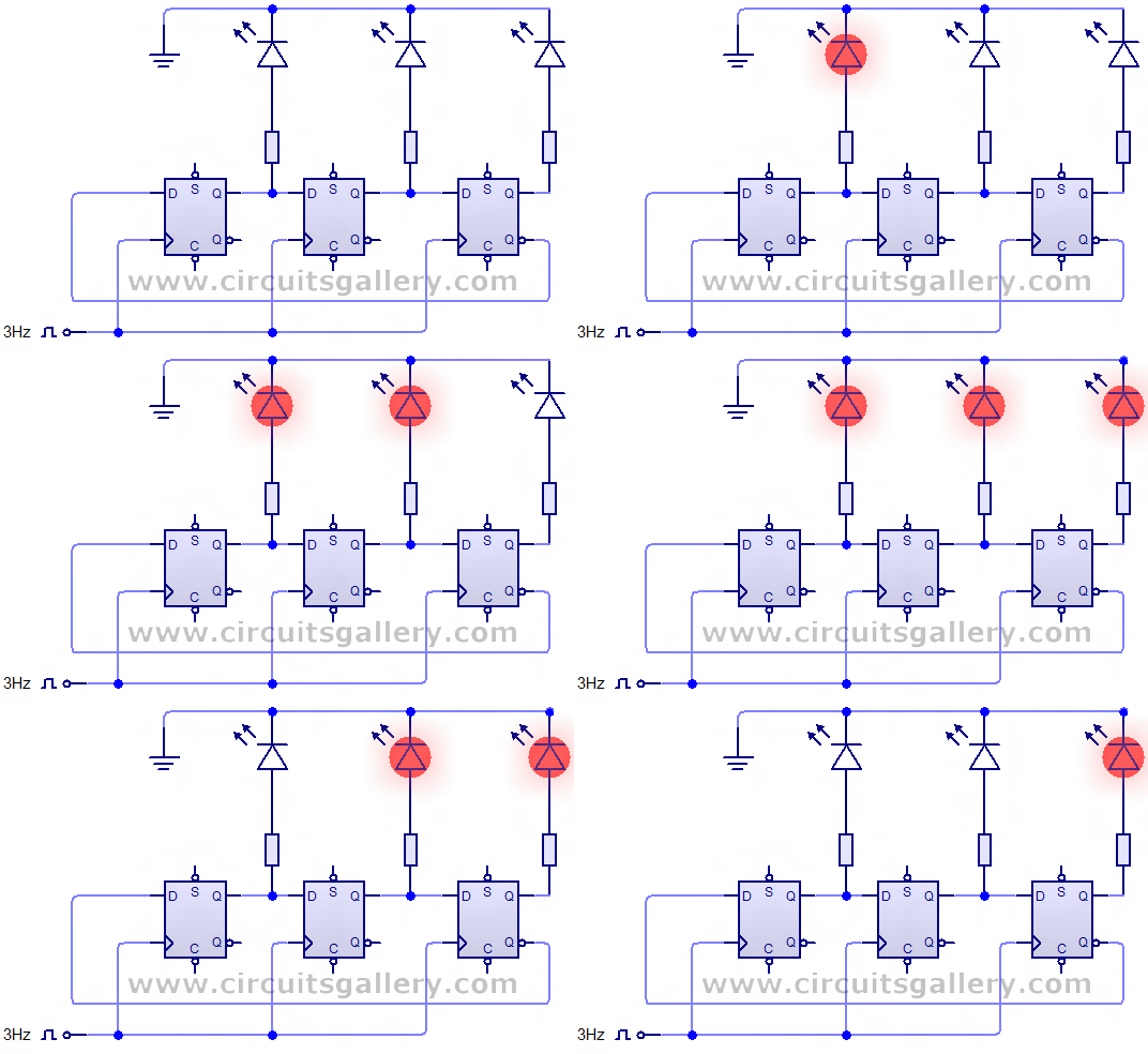
        circuit diagram represents a 3 bit Johnson counter using 7474 D flip flop. You can easily extent this     circuit up to 4 bit, 5 bit, etc. by adding flip flops after 3rd flips flop.

  • A single 7474 IC consist of 2 flip flops so you need two 7474 ICs for implementing Johnson counter.
  • Initially all the flip flops are cleared, so the time inverted output (Q’) of 3rd flip flop is high or logic 1.
  • This logic 1 is appears at the input of 1st flip flop. During the first clock pulse this logic 1 is transferred to the output of 1st flip flop. Thus the total output of Johnson counter is 100.
  • Then input of 1st and 2nd flip flop is logic 1 and after the second clock pulse these inputs appear at the outputs of 1st and 2nd flip flop. So the total output is 110.
  • Similarly for the next clock pulse, the output will be 111.
  • During this state (111) the time inverted output (Q’) is logic 0. This 0 is fed to the 1st flip flop. Then the 0 will circulate through the flip flops as 011,001,000.                                                         

Transistor acts as a switch

The above shown the working of transistor as a switch..


Hardwork can never ever fails..
Best Luck...

N-channel JFET -Working Animation

Click below to view the animation
Working Animation


Hardwork Can Never Ever Fails...
Best Luck..

N channel Enhancement MOSFET-Working Animation

Click Below
Working Animation


Hardwork Can Never Ever Fails...
Best Luck...

Wednesday, July 11, 2012

555 TIMER


A 555 timer is a type of integrated circuit, also known as a chip, which is extremely popular for a variety of purposes. Its main use is as a timer, but it can also be used as a multivibrator.

The 555 timer takes its name from the fact that the original model had three resistors each rated at five thousand ohms. The first model was formally known as the SE555/NE555 and marketed as the IC Time Machine. At the time of its 1971 release, the 555 timer was the only commercially available timer circuit. Today there are many different models from different companies, though nearly all manufacturers include 555 as part of the model number because it’s such a recognizable name.
There are two different types of 555 timer, both being eight-pin chips. The most common one is the rectangular ‘V’ package, which has four pins down each side. The other version, which used to be the most common but has now fallen from favor somewhat, is the circular ‘T’ package.
The eight pins carry out the following functions:
  1. Ground, which acts as a safety measure as with electrical plugs
  2. Trigger, which passes on voltage to start the timing operations
  3. Output, which carries voltage to the device using the timer
  4. Reset, which is used to end the timing operation
  5. Control voltage, an optional pin used for controlling the timer from outside the main circuit set-up
  6. Threshold, which determines how long the timer should output voltage in each on/off cycle – in other words, how long the timing interval should be
  7. Discharge, connected to a capacitor which also influences the timing interval
  8. V+, which is the voltage input
There are three different types of use for a 555 timer. Monostable operation is when the output signal simply switches between the default off position and a temporary on position at regular intervals, which is most commonly used for timers. Astable operation is when the output voltage rises and falls in a set pattern, making it an oscillator. As the pattern can be varied, it can be used for any purpose which requires a particular tone pattern. Bistable operation is when the signal can be held in one of two positions, meaning the 555 timer can act as the smallest possible unit of computer memory.


Tuesday, July 10, 2012

4 bit ripple counter working Animation

Ripple Counter

               An asynchronous (ripple) counter is a single JK-type flip-flop, with its J (data) input fed from its own inverted output. This circuit can store one bit, and hence can count from zero to one before it overflows (starts over from 0). This counter will increment once for every clock cycle and takes two clock cycles to overflow, so every cycle it will alternate between a transition from 0 to 1 and a transition from 1 to 0. Notice that this creates a new clock with a 50% duty cycle at exactly half the frequency of the input clock.

Click below to see the animation

 Ripple Counter

Hardwork Can  never Ever Fails...

Best Luck...

Monday, July 09, 2012

Binary Decoder working Animation

Click Below:

Binary Decoder animation

Hardwork Can Never Ever  Fails..
Best Luck..

Brige Rectifier Working animation

Click Below:
Bridge Rectifier

Hardwork Can Never Ever Fails...
Best Luck..

High Pass Filter -working and Animation

Click Below to see the animation of high pass filter
High pass filter animation


Hardwork Can Never Ever Fails...
Best Luck...

Time Division Multiplexing-Animation

TDM:

     Time division multiple access (TDMA) is a channel access method for shared medium networks. It allows several users to share the same frequency channel by dividing the signal into different time slots.

Click Below to see the animation:


Hardwork Can Never Ever Fails..
Best Luck...

Quadrature amplitude modulation-Animation

QAM:

       Quadrature amplitude modulation (QAM)  is both an analog and a digital modulation scheme. It conveys two analog message signals, or two digital bit streams, by changing (modulating) the amplitudes of two carrier waves, using the amplitude-shift keying (ASK) digital modulation scheme or amplitude modulation (AM) analog modulation scheme. The two carrier waves, usually sinusoids, are out of phase with each other by 90° and are thus called quadrature carriers or quadrature components — hence the name of the scheme. The modulated waves are summed, and the resulting waveform is a combination of both phase-shift keying (PSK) and amplitude-shift keying (ASK), or (in the analog case) of phase modulation (PM) and amplitude modulation.

Click below to view the animation :

Hardwork Can Never Ever Fails..
Best Luck...

Pulse code modulation-Animation

PCM

              Pulse-code modulation (PCM) is a method used to digitally represent sampled analog signals. It is the standard form for digital audio in computers and various Blu-ray, DVD and Compact Disc formats, as well as other uses such as digital telephone systems. A PCM stream is a digital representation of an analog signal, in which the magnitude of the analog signal is sampled regularly at uniform intervals, with each sample being quantized to the nearest value within a range of digital steps.


click below to see the animation :

pcm animation

Hardwork Can Never Ever fails...
Best Luck...

Pulse Amplitude Modulation-Animation

PAM 

     Pulse-amplitude modulation, acronym PAM, is a form of signal modulation where the message information is encoded in the amplitude of a series of signal pulses. It is an analog pulse modulation scheme in which the amplitude of train of carrier pulse are varied according to the sample value of the message signal.

Click below to see the animation


Hardwork Ever Never Fails...
Best Luck...

Amplitude Shift Keying (ASK)-Animation

ASK:

    Amplitude-shift keying (ASK) is a form of modulation that represents digital data as variations in the amplitude of a carrier wave.

Click below to view the animation

ASK animation

Hardwork Can Never Ever Fails..
Best Luck...
   

Basic Modulation Techniques -Animation

Click below to see the animation of  AM,PM,FM
Modulation animations


Hardwork Can Never Ever fails...
Best Luck...

One More Explanation of How a Transistor Works.

Transistor Working

Operation of JFET Animation


Animation of JFET:

Direction of Electron Motion Animation


 Direction of electron motion:


Yahoo

Sunday, July 08, 2012

Full wave bridge rectifier working and animation

Click below to see the working animation
Bridge rectifier


Hardwork can never ever fails...
Good Luck....

Demultiplexer-Detailed animation

Click below to see the detailed animation of Demux
Demux animation


Hardwork Never ever fails...
Best Luck...

Mutiplexer-Detailed animation

Click below to view the multiplexer animation
Multiplexer animation


Hardwork Never ever fails....
Best Luck....

SR flip flop animation

SR Flip Flop

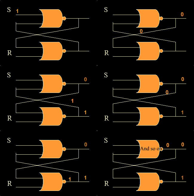
When using static gates as building blocks, the most fundamental latch is the simple SR latch, where S and R stand for set and reset. It can be constructed from a pair of cross-coupled NORlogic gates. The stored bit is present on the output marked Q.

While the S and R inputs are both low, feedback maintains the Q and Q outputs in a constant state, with Q the complement of Q. If S (Set) is pulsed high while R (Reset) is held low, then the Q output is forced high, and stays high when S returns to low; similarly, if R is pulsed high while S is held low, then the Q output is forced low, and stays low when R returns to low.

SET operation

RESET operation


H

Hardwork Never ever fails...

Best Luck...

Saturday, July 07, 2012

Full adder animation

Full adder

        A full adder adds binary numbers and accounts for values carried in as well as out. A one-bit full adder adds three one-bit numbers, often written as A, B, and Cin; A and B are the operands, and Cin is a bit carried in from the next less significant stage.
        

Full adder animation


Hardwork never ever fails...
Best Luck...

Relay Working

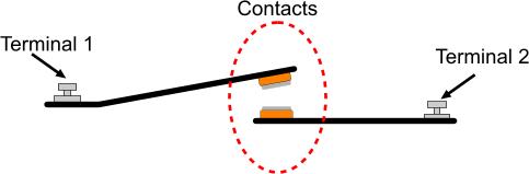
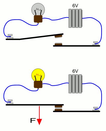
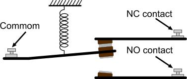
Each relay has two mechanical parts inside. The first one is the contact(s) of the relay. The contacts operates similarly to the contacts of a simple switch or pushbutton. You should consider the contacts as a pair of metals like the following diagram:


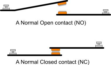
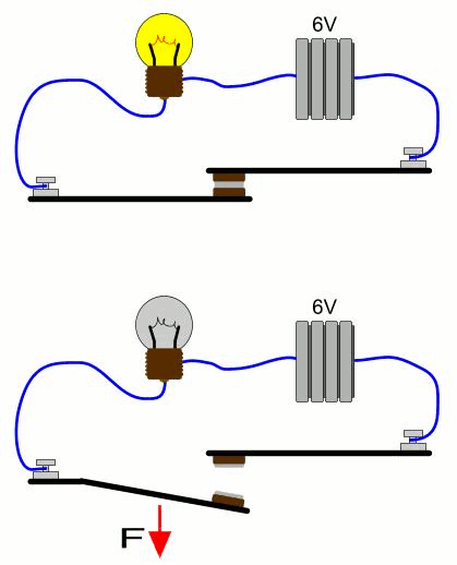
The two terminals operates as a switch. When the contacts are 'in contact' then the current flows from Terminal 1 to Terminal 2. There are two types of contacts: the NO and the NC. NO stands for Normal Open contact, while NC stands for Normal Closed contact. The Normal Open is a contact like the one showed in the previous illustration. When the contact is still, then no current flows through it (because it is an OPEN circuit). On the other hand, a Normal Closed contact allows the current to flow when the contact is still. Bellow i illustrate both of these contacts:


You may notice that the NC contact is turned upside-down compared to the NO contact. This is done in purpose. This way, both contacts (NO and NC) will change state if a force is applied to the left metal heading from UP to DOWN. The following animation shows how a NO contact operates by lighting a light bulb:


As for the NC contacts, it works exactly opposite as the NO contacts. Look the following animation:


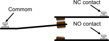
A combination of contacts

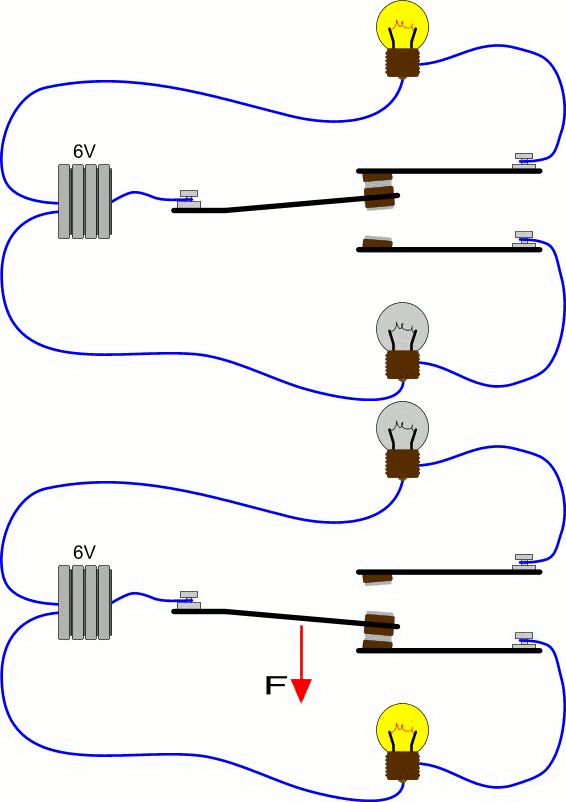
A relay may have a combination of the above contacts. Look at the following illustration


In this case, there is a 3rd terminal called "COMMON". The NO and NC contacts are referred to the COMMON terminal. Between the NC and the NO contact, there is no contact at any time! The following animation shows how this pair operates:


And WHO defines the NORMAL state?

OK, we have the NORMAL open and NORMAL closed contact. But which state is considered as NORMAL? Going one step closer to the relay operation, we find the spring. This spring defines the NORMAL position of the COMMON contact. If you see the above 3 animations, you will notice that one time an F force is applied to the COMMON terminal, and the other time there is no force applied. Well, this is actually wrong. There is indeed another force that pulls the contact towards UP and this force is applied ALL the time. This force comes from the spring. Look the following image:


Now you can see who is pulling the COMMON terminal UP all the time. So the spring defines what is the NORMAL state, and thus defines which contact is the NORMAL OPEN and which the NORMAL CLOSED. In other words, the NORMAL state is defined as the state that there is NO other force applied to the COMMON terminal except the one from the spring.


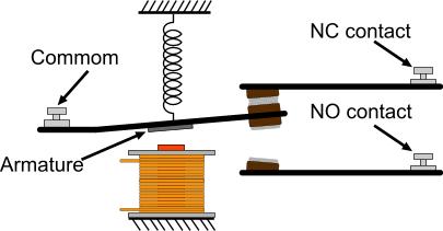
The last part - WHO move the common contact of the relay?

This is the last part of the relay operation. The device that forces the terminal to move, is actually an electromagnet! A coil is placed right under the contact. When current is flown through this coil, a magnetism is created. This magnetism can overcome the force of the spring and can pull the contact towards it, thus it changes it's position! And due to the fact that the contact is usually a small piece of metal not capable to be pulled by the electromagnet, another piece of metal is attached to the common. This piece of metal is so called "Armature". Following is (at last) the complete illustration of the basic relay:


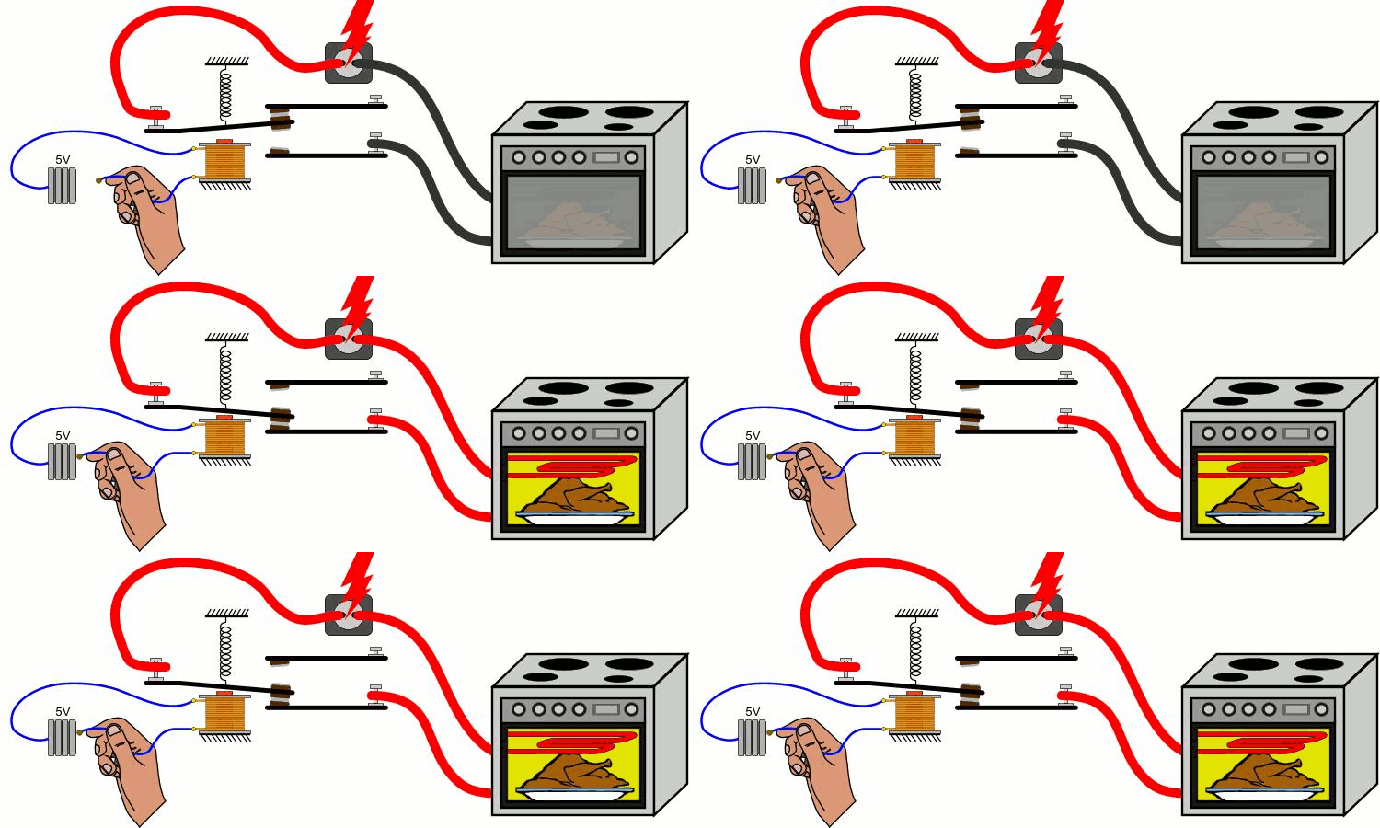
Now, imagine that someone wants to control a 220Volts 1 K-Watt load with a command that comes from a 5 Volts battery. A load-Relay should be used for this application. The Coil of the relay is driven with the 5 Volts. The contacts from this relay (NO) will be connected in series with the power supply of the load. Thus, the load will only operate when the relay is actuated. Our friend bellow will turn on an electric oven bare-handed!!!


NPN Transistor Operation

NPN- Transistor Operation

A forward-biased pn- junction is comparable to a low-resistance circuit element because it passes a high current for a given voltage. In turn, a reverse-biased pn- junction is comparable to a high-resistance circuit element. By using the Ohm's law formula for power (P = I2·R) and assuming current is held constant, you can conclude that the power developed across a high resistance is greater than that developed across a low resistance. Thus, if a crystal were to contain two pn- junctions (one forward-biased and the other reverse-biased), a low-power signal could be injected into the forward-biased junction and produce a high-power signal at the reverse-biased junction. In this manner, a power gain would be obtained across the crystal. This concept, which is merely an extension of the material covered in the previous topics, is the basic theory behind how the transistor amplifies. With this information fresh in your mind, let's proceed directly to the npn transistor.


The forward-biased junction in an npn- transistor
The forward-biased junction in an npn transistor


Just as in the case of the pn- junction diode, the n- material comprising the two end sections of the npn transistor contains a number of free electrons, while the center p section contains an excess number of holes. The action at each junction between these sections is the same as that previously described for the diode; that is, depletion regions develop and the junction barrier appears. To use the transistor as an amplifier, each of these junctions must be modified by some external bias voltage. For the transistor to function in this capacity, the first pn- junction (emitter-base junction) is biased in the forward, or low-resistance, direction. At the same time the second pn- junction (base-collector junction) is biased in the reverse, or high-resistance, direction. The letters of these elements indicate what polarity voltage to use for correct bias. For instance, notice the npn transistor shown in figure 2:

The emitter, which is the first letter in the npn sequence, is connected to the negative side of the battery while the base, which is the second letter (npn), is connected to the positive side. However, since the second pn- junction is required to be reverse biased for proper transistor operation, the collector must be connected to an opposite polarity voltage (positive) than that indicated by its letter designation (npn). The voltage on the collector must also be more positive than the base, as shown beside:

We now have a properly biased npn transistor.

In summary, the base of the npn transistor must be positive with respect to the emitter, and the collector must be more positive than the base.

The junctions in an npn transistor.
The junctions in an npn transistor.

npn forward-biased junction


An important point to bring out at this time, which was not necessarily mentioned during the explanation of the diode, is the fact that the n- material on one side of the forward-biased junction is more heavily doped than the p material. This results in more current being carried across the junction by the majority carrier electrons from the n- material than the majority carrier holes from the p material. Therefore, conduction through the forward-biased junction, as shown in figure 3, is mainly by majority carrier electrons from the n- material (emitter).
Currents around the forward-biased junction in an npn transistor.
Currents around the forward-biased junction in an npn transistor.

With the emitter-to-base junction in the figure biased in the forward direction, electrons leave the negative terminal of the battery and enter the n- material (emitter). Since electrons are majority current carriers in the n- material, they pass easily through the emitter, cross over the junction, and combine with holes in the p material (base). For each electron that fills a hole in the p material, another electron will leave the p material (creating a new hole) and enter the positive terminal of the battery.
 
 npn reverse-biased junction
The reverse-biased junction in an npn transistor
The reverse-biased junction in an npn transistor.


The second pn- junction (base-to-collector), or reverse-biased junction as it is called (figure 4), blocks the majority current carriers from crossing the junction. However, there is a very small current, that does pass through this junction. This current is called minority current, or reverse current. As you recall, this current was produced by the electron-hole pairs. The minority carriers for the reverse-biased pn- junction are the electrons in the p material and the holes in the n- material. These minority carriers actually conduct the current for the reverse-biased junction when electrons from the p material enter the n material, and the holes from the n- material enter the p- material. However, the minority current electrons play the most important part in the operation of the npn transistor.
 
npn- junction interaction
The bias batteries in the figure 5 have been labeled VCC for the collector voltage supply, and VBB for the base voltage supply. Also notice the base supply battery is quite small, as indicated by the number of cells in the battery, usually 1 volt or less. However, the collector supply is generally much higher than the base supply, normally around 6 volts. This difference in supply voltages is necessary to have current flow from the emitter to the collector.

npn transistor operation
npn transistor operation is basically the action of a relatively small emitter-base bias voltage controlling a relatively large emitter-to-collector current.


The current flow in the external circuit is always due to the movement of free electrons. Therefore, electrons flow from the negative terminals of the supply batteries to the n-type emitter. This combined movement of electrons is known as emitter current (IE). Since electrons are the majority carriers in the n- material, they will move through the n- material emitter to the emitter-base junction. With this junction forward biased, electrons continue on into the base region. Once the electrons are in the base, which is a p-type material, they become minority carriers. Some of the electrons that move into the base recombine with available holes. For each electron that recombines, another electron moves out through the base lead as base current IB (creating a new hole for eventual combination) and returns to the base supply battery V.

The electrons that recombine are lost as far as the collector is concerned. Therefore, to make the transistor more efficient, the base region is made very thin and lightly doped. This reduces the opportunity for an electron to recombine with a hole and be lost. Thus, most of the electrons that move into the base region come under the influence of the large collector reverse bias. This bias acts as forward bias for the minority carriers (electrons) in the base and, as such, accelerates them through the base-collector junction and on into the collector region. Since the collector is made of an n-type material, the electrons that reach the collector again become majority current carriers. Once in the collector, the electrons move easily through the n material and return to the positive terminal of the collector supply battery VCC as collector current (IC).

To further improve on the efficiency of the transistor, the collector is made physically larger than the base for two reasons: (1) to increase the chance of collecting carriers that diffuse to the side as well as directly across the base region, and (2) to enable the collector to handle more heat without damage.

Total current flow in the npn transistor


In summary, total current flow in the npn transistor is through the emitter lead. Therefore, in terms of percentage, IE is 100 percent. On the other hand, since the base is very thin and lightly doped, a smaller percentage of the total current (emitter current) will flow in the base circuit than in the collector circuit. Usually no more than 2 to 5 percent of the total current is base current (IB) while the remaining 95 to 98 percent is collector current (IC). A very basic relationship exists between these two currents:

IE = IB + IC

In simple terms this means that the emitter current is separated into base and collector current. Since the amount of current leaving the emitter is solely a function of the emitter-base bias, and because the collector receives most of this current, a small change in emitter-base bias will have a far greater effect on the magnitude of collector current than it will have on base current. In conclusion, the relatively small emitter-base bias controls the relatively large emitter-to-collector current.

Comparator Animation

What is Comparator?

In electronics, a comparator is a device that compares two voltages or currents and switches its output to indicate which is larger. They are commonly used in devices such as Analog-to-digital converters (ADCs).


Comparator animation


Hardwork Never Ever Fails...
Best Luck...

AND & OR gates with switch-animation


AND & OR


Hardwork never ever fails...
Best Luck....

555 timer working and animation

what is 555 timer?


The 555 timer IC is an integrated circuit (chip) used in a variety of timer, pulse generation, and oscillator applications. The 555 can be used to provide time delays, as an oscillator, and as a flip-flop element. Derivatives provide up to four timing circuits in one package.

Circuit Connection:

        The IC is available in either an 8-pin round TO3-style can or an 8-pin mini-DIP package.


    1. Ground.
    2. Trigger input. 
    3. Output. 
    4. Reset input. 
    5. Control voltage. 
    6. Threshhold input. 
    7. Discharge. 
    8. +VCC. +5 to +15 volts in normal use. 

Working:

1.The 3 resistors across the power supply forms a voltage divider and the two comparator is connected to it.The IC is quiescent so long as the trigger input (pin 2) remains at +VCC and the threshhold input (pin 6) is at ground. Assume the reset input (pin 4) is also at +VCC and therefore inactive, and that the control voltage input (pin 5) is unconnected. Under these conditions, the output (pin 3) is at ground and the discharge transistor (pin 7) is turned on, thus grounding whatever is connected to this pin.

2.The three resistors in the voltage divider all have the same value (5K in the bipolar version of this IC), so the comparator reference voltages are 1/3 and 2/3 of the supply voltage, whatever that may be. The control voltage input at pin 5 can directly affect this relationship, although most of the time this pin is unused.

3.The internal flip-flop changes state when the trigger input at pin 2 is pulled down below +VCC/3. When this occurs, the output (pin 3) changes state to +VCC and the discharge transistor (pin 7) is turned off. The trigger input can now return to +VCC; it will not affect the state of the IC.

Modes:

       The 555 can operate in either monostable or astable mode, depending on the connections to and the arrangement of the external components. Thus, it can either produce a single pulse when triggered, or it can produce a continuous pulse train as long as it remains powered.

Animation Below: 

555 timer animation

Hardwork Never Ever Fails...
Best Luck....


Thursday, July 05, 2012

Different Types of Diodes

Types of Diodes:

Small signal or Small current diode - These diodes assumes that the operating point is not affected because the signal is small.


Large signal diodes - The operating point in these diodes get affected as the signal is large.


Zener diodes - This diode runs in reverse bias condition when the voltage reaches the breakdown point. A stable voltage can be achieved by placing a resistor across it to limit the current. This diode is used to provide reference voltage in power supply circuits.


Light emitting diodes (LED) - This is the most popular kind of diode.When it works in the forward bias condition, the current flows through the junction to produce the light.


Photodiodes - The electrons and holes are generated as light strikes across the p-n junction causing the current to flow. Theses diodes can work as photodetector and are used to generate electricity.


Constant current diodes - This diode keeps the current constant even when the voltage applied keeps changing. It consists of JFET (junction – field effect transistor) with the source shorted to the gate in order to function like a two - terminal current limiter or current source.


Schottky diode - These diodes are used in RF applications and clamping circuits. This diode has lower forward voltage drop as against the silicon PN junction diodes.


Shockley diode - This is a four layer diode which is also known as PNPN diode. This diode is similar to thyristor where the gate is disconnected.


Step recovery diodes - This semiconductor diode has the ability to generate short pulses and hence it is used in microwave applications as a pulse generator.


Tunnel diodes - This diode is heavily doped in the forward bias condition that has a negative resistance at extremely low voltage and a short circuit in the negative bias direction. This diode is useful as a microwave amplifier and in oscillators.


Varactor diodes - This diode works in reverse bias condition and restricts the flow of current through the junction. Depending on the amount of biasing, the width of the depletion region keeps varying. This diode comprises of two plates of a capacitor with the depletion region amidst them. The variation in capacitance depends upon the depletion region and this can varied by altering the reverse bias on the diode.


PIN diodes - This diode has intrinsic semiconductor sandwiched between P- type and N- type region. Doping does not occur in this type of diode and thereby the intrinsic semiconductor increases the width of the depletion region. They are used as ohtodiodes and radio frequency switches.


LASER diode - This diode produces laser type of light and are expensive as compared to LED. They are widely used in CD and DVD drives.


Transient voltage supression diodes - This diode is used to protect the electronics that are sensitive against voltage spikes.


Gold doped diodes - These diodes use gold as the dopant and can operate at signal frequencies even if the forward voltage drop increases.


Super barrier diodes - These are also called as the rectifier diodes. These diodes have the property of low reverse leakage current as that of normal p-n junction diode and low forward voltage drop as that of Schottky diode with surge handling ability.


Point contact diodes - The construction of this diode is simpler and is used in analog applications and as a detector in radio receivers. This diode is built of n – type semiconductor and few conducting metals placed to be in contact with the semiconductor. Some metals move from towards the semiconductor to form small region of p- type semiconductor near the contact.


Peltier diodes - This diode is used as heat engine and sensor for thermoelectric cooling.


Gunn diode - This diode is made of materials like GaAs or InP that exhibit a negative differential resistance region.


Crystal diode - These are a type of point contact diodes which are also called as Cat’s whisker diode. This diode comprises of a thin sharpened metal wire which is pressed against the semiconducting crystal. The metal wire is the anode and the semiconducting crystal is the cathode. These diodes are obsolete.


Avalanche diode - This diode conducts in reverse bias condition where the reverse bias voltage applied across the p-n junction creates a wave of ionization leading to the flow of large current. These diodes are designed to breakdown at specific reverse voltage in order to avoid any damage.


Silicon controlled rectifier - As the name implies this diode can be controlled or triggered to the ON condition due to the application of small voltage. They belong to the family of Thyristors and is used in various fields of DC motor control, generator field regulation, lighting system control and variable frequency drive. This is three terminal devices with anode, cathode and third controlled lead or gate.


Vaccum diodes - This diode is two electrode vacuum tube which can tolerate high inverse voltages.

Capacitor and DC

Capacitor will not conduct DC Current. LED comes on very briefly when the switch is closed to show the capacitor is charging. But after the initial charge, the LED does not illuminate.


(Courtesy: talkingelectronics.com)

See the below animation
Capacitor and DC

Charging a Capacitor

How to charge a capacitor?

When a voltage is connected to a capacitor it charges up. It's a bit like charging the battery in your mobile phone. In fact the mobile phone battery can be considered to be a very large capacitor.

(Courtesy: talkingelectronics.com)

See the below animation.
Charging a Capacitor


Charging a Capacitor- Characteristics

Resistor and Current Flow

How the resistor in a circuit affects the current flow through the circuit??

A low value resistor is like a thick pipe - lots of water flows - lots of current flows. A high value resistor is like a pipe with a restriction - little water flows - only a low current will flow.

(Courtesy: talkingelectronics.com)


See the below animation.
Water flow-Circuit analogy

Monday, July 02, 2012

Micro Processor


A fantastic collection of Microprocessor basics is available as interactive animations in the following link.


Please Click Here to view the animations.


I am sure that it will be helpful for us to understand, how the data and instruction flow is taking place in the Microprocessor...